
The start-up raised $50 million in 2025, funding that will move the company from pilot shipments to high-volume manufacturing of its optical input-output (I/O) interface technology.
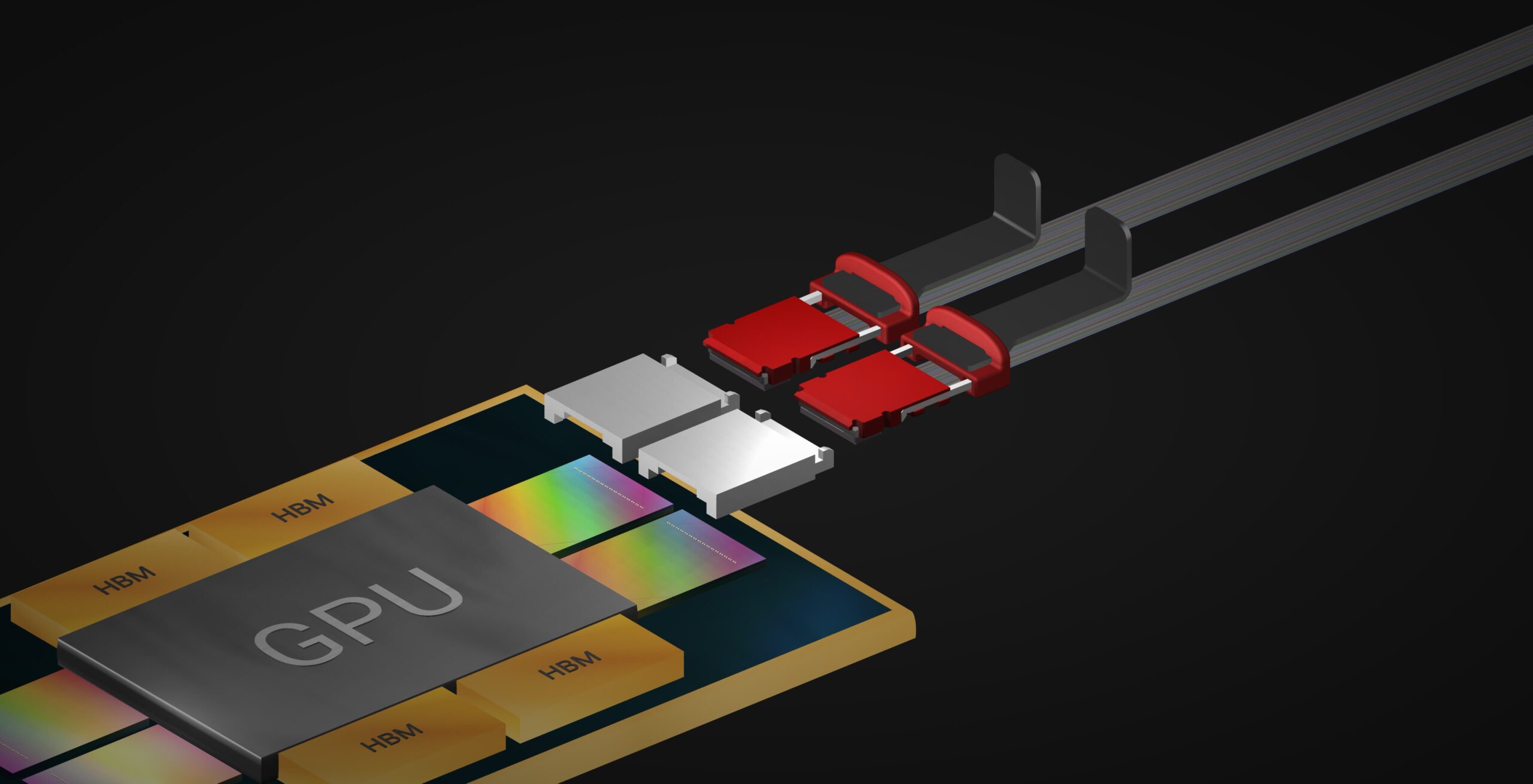
Teramount is advancing its fibre-to-chip coupling technology toward volume manufacturing. The start-up is targeting the emerging co-packaged optics (CPO) market, where photonics is integrated directly with a chip to improve speed and energy efficiency.
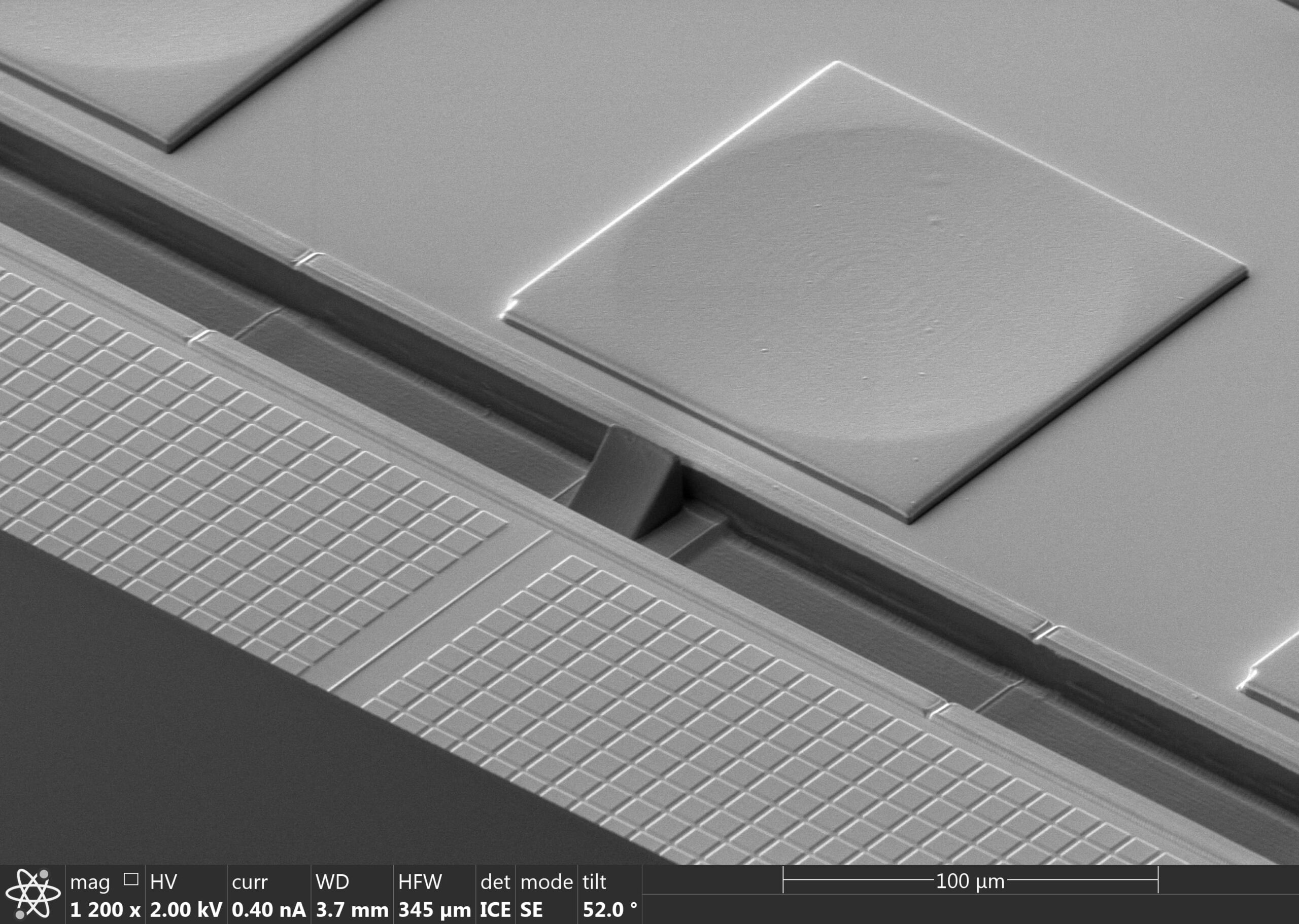
The company has developed a way to attach fibres to a chip suited to semiconductor manufacturing.
The start-up’s focus is to match its interface to the process steps across the supply chain—at photonic chip foundries and outsourced semiconductor assembly and test (OSAT) houses.
The $50 million funding advances Teramount’s plans, says Hesham Taha, CEO of Teramount, to enable optical connectivity for use in advanced AI computing systems.
Wideband surface coupling
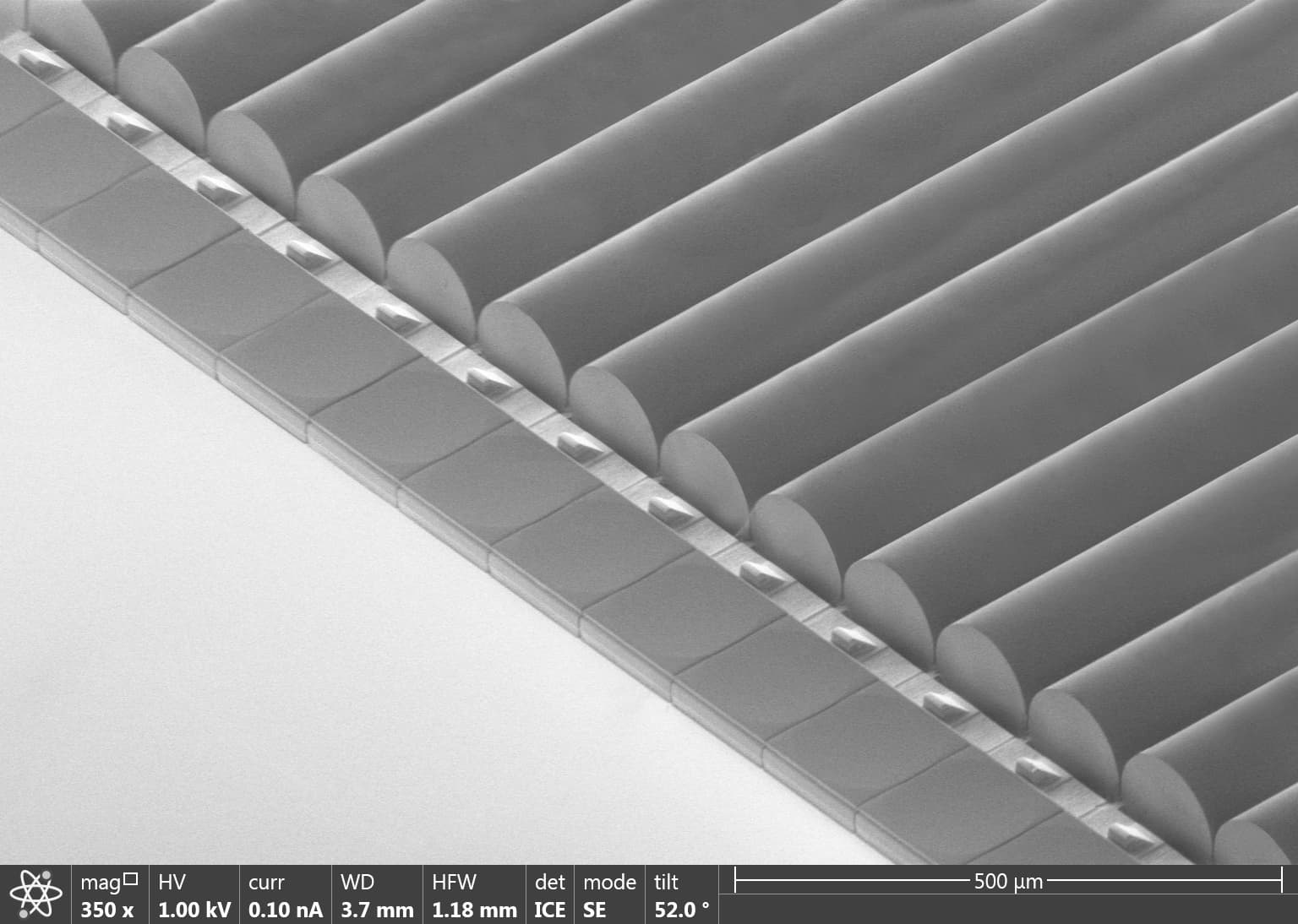
Teramount’s core intellectual property connects fibre to a chip’s surface without the bandwidth penalties associated with conventional surface coupling.
In silicon photonics, “surface coupling” is often shorthand for a grating coupler. Teramount’s approach uses what it calls a photonic bump — a coupling and packaging construct integrated into a semiconductor-style process flow — that delivers a wide optical bandwidth with the advantages of surface-mount packaging.
Surface coupling is attractive to photonic chip designers because it eases some of the geometric and packaging constraints of attaching fibres to a chip’s edge. This is becoming more important as systems push toward higher aggregate fibre counts, denser packaging, and tighter link budgets.
Teramount argues that its bump-based approach can reduce the bandwidth/efficiency trade-offs that start to dominate when designers scale fibre counts and power budgets.
“Our philosophy has been that we needed to bring optics to speak the same language as semiconductor manufacturing,” says Taha. “This is the purpose of our photonic bump.”
Product and positioning
Companies are evaluating Teramount’s TeraVERSE surface-mount fibre-attach product which is now sampling.
Teramount is pursuing more than one on-ramp into silicon photonics packaging and says its approach supports co-packaged optics for scale-out and for scale-up architectures once the industry is ready to replace copper interconnects with optics for short reaches (1-3m).
The start-up has a roadmap that enables fibre stacking to increase attach density—an important lever in co-packaged optics-where fibre routing becomes a constraint.
The company says its units are being integrated into silicon photonics wafers at multiple foundries, assembled at major OSATs, and delivered through partner and customer flows aimed at co-packaged optics programmes.
Such integration is challenging. Once optics moves inside advanced packages, alignment tolerances, reflow compatibility, thermal and mechanical stress, and test strategy, all must be addressed in a production setting. Teramount argues the ecosystem is learning these lessons in real time, with system requirements evolving rapidly.
“Customers are asking to increase the number of fibres, increase the optical power, and meet harsh environmental conditions,” says Taha. “Every vendor needs to accommodate these changes on the go.”
Taha also highlights other challenges: fibre management inside the system, accommodating single-mode and polarisation-maintaining fibre where required, and the practical question of “who owns what” when optics meets the chip industry’s established division of responsibilities.
New customers used to volumes
For Teramount, the most consequential change is the nature of the customer. When leading semiconductor companies—AI accelerator and switching players—come to a foundry with a co-packaged optics requirement, it forces engagement at a different level than photonics start-ups can drive.
“The main change is the ownership of the co-packaged optics,” says Taha. “It’s a chip company that is now coming to a foundry for co-packaged optics—and the volumes are going to be high.”
By volume, the expectation is millions of units per year. The company says it is targeting that capability for the middle of 2027.
This shift matters because foundry process tweaks, OSAT line development, supply-chain readiness, and reliability qualification move faster when a high-volume chip programme is the driver.
Manufacturing ramp
Teramount’s Series A funding is aimed at accelerating production plans, expanding suppliers and foundry engagements, and building internal capability to manage a volume transition.
Today, the company operates a pilot-line approach that uses distributed equipment across local and global suppliers, but Teramount is moving toward a consolidated and scalable flow. “We are gathering equipment to have the line in one place,” says Taha.
Teramount says it has grown its staff by half in 2025 to 60, with hiring focussed on operations and manufacturing expertise aligned with high-volume semiconductor making.
There is no one standard for co-packaged optics but eventually the market will settle on a de facto approach, says Taha.
Teramount is effectively betting that manufacturing readiness is a differentiator—and that wideband surface coupling, if it can be packaged and produced like microelectronics – can be part of the co-packaged optics wave that will ship at scale.
Meanwhile, Teramount is aligned with what a key industry transition looks like: a $50 million funding round pointing straight at an important volume manufacturing bottleneck.
Backers of Teramount’s Series A funding round include Koch Disruptive Technologies (KDT), AMD Ventures, Hitachi Ventures, Samsung Catalyst Fund, Wistron, and Grove Ventures.