
Ayar Labs progresses towards volume manufacturing of its TeraPHY optical input-output (I/O) chiplet.
It is a decade since Vladimir Stojanovic was co-author of a paper published in the science journal, Nature, outlining the first microprocessor to send and receive data optically.
“For the first time, a system – a microprocessor – has been able to communicate with the external world using something other than electronics,” said Stojanovic, then an associate professor of electrical engineering and computer science at the University of California, Berkeley
Ten years on, silicon photonics and optics packaged alongside silicon have come a long way.
Broadcom has added its third-generation co-packaged optics design to its 102.4 Terabit-per-second (Tbps) Tomahawk 6 switch chip. And Nvidia has announced two families of switches, its first, that use the optical technology.
Co-packaged optics has long been promoted as lowering power consumption and aiding processing scalability. But in the last year it has proven to be far more reliable than traditional pluggable optics.
Ayar Labs, too, has come a long way, a start-up Stojanovic co-founded and which, since 2024, has been its chief technology officer (CTO). In 2025, Ayar Labs detailed its third-generation TeraPHY optical I/O chiplet, first in a post-deadline paper at OFC 2025 and then at the Hot Chips 2025 event this summer.
The start-up has also announced partnerships with Taiwanese ASIC design companies, Alchip Technologies and Global Unichip Corp (GUC), both with strong links with leading foundry, TSMC.
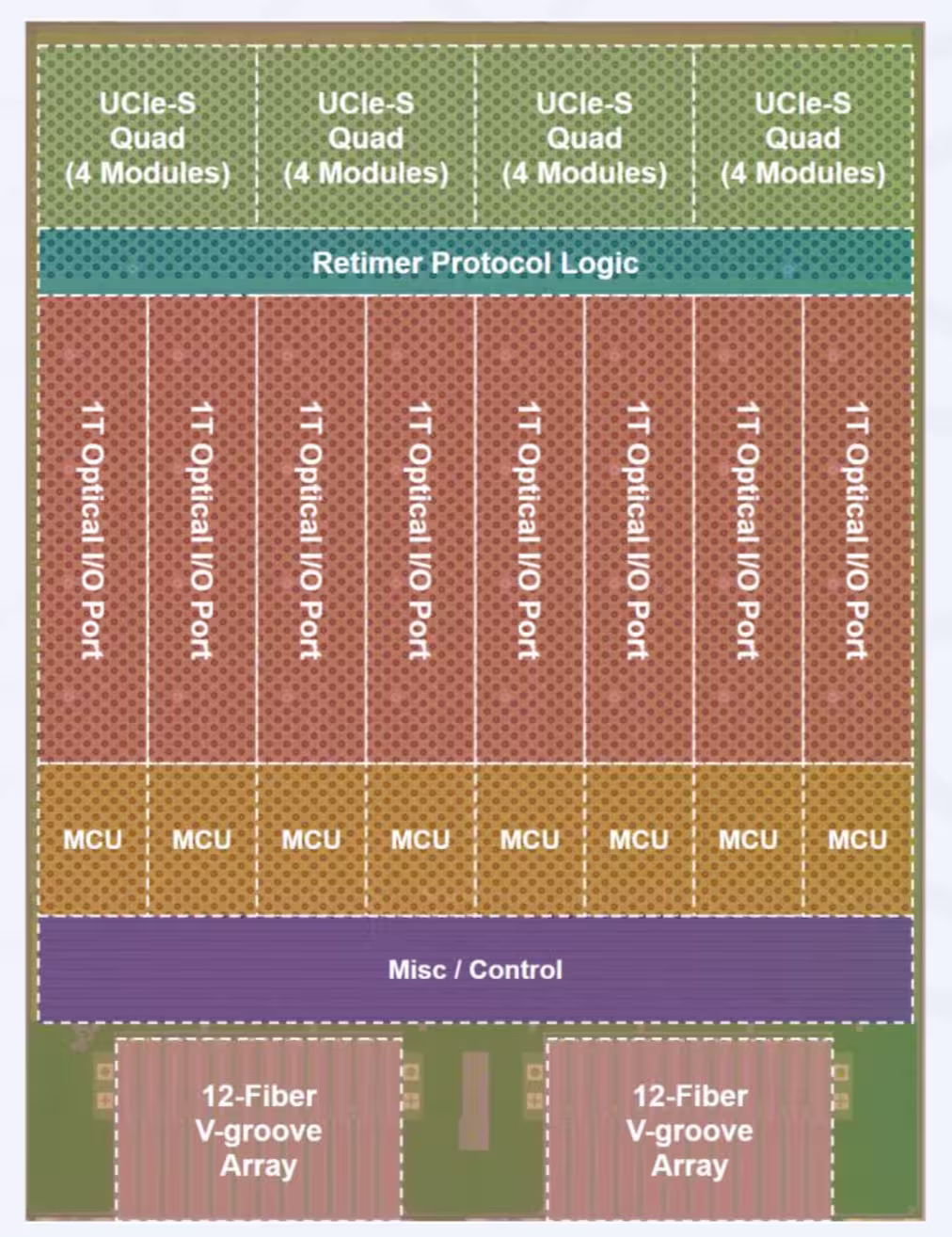
Third-generation TeraPHY optical I/O chiplets
The latest TeraPHY optical I/O chiplet has a bidirectional bandwidth of 8Tbps, or 4Tbps in each direction (see diagram above). It is also the first chiplet design to carry Universal Chiplet Interconnect Express (UCIe) traffic optically. UCIe is a standard die-to-die protocol and Ayar Labs has extended its reach using light. UCIe can carry various protocols and Stojanovic describes the latest device as a ‘universal I/O chiplet’.
The chiplet uses eight 1Tbps optical ports, each supporting 512Gbps channels per direction. Each wavelength carries a 32Gbps signal and using 16 silicon photonics micro-ring resonators, there are 16 wavelengths per fibre.
Ayar Labs also makes a custom-designed laser module – the external light source – that powers the TeraPHY optical I/O chiplets. Dubbed the SuperNova light source, the module uses an array of distributed feedback (DFB) lasers provided by Sivers Photonics.
Ayar Labs uses Sivers’ DFB cell and has adapted it to create a laser array packaged in a module, with the lasers multiplexed and split into wavelengths.
A SuperNova module can have 8 or 16 ports, each with 16 wavelengths, for a total of 128 or 256 wavelengths.
From monolithic optics to modular chiplets
Ayar Labs is a fabless company, meaning it can choose a fab for its design to deliver the best performance and cost. “And in an appropriate ecosystem where our customers want to build their solutions,” adds Stojanovic.
“This [TeraPHY optical I/O chiplet] architecture lets us move seamlessly through different foundry processes,” says Stojanovic. “We can adopt the best CMOS node for logic while keeping the photonic building blocks stable.”
The 8Tbps TeraPHY device is built using GlobalFoundries’ 45SPCLO 45nm silicon-photonics process — a platform that Ayar Labs helped shape. But the design can also be migrated to TSMC’s more advanced CMOS nodes for the electrical IC while benefiting from TSMC’s silicon photonics and packaging flows.
Universal I/O chiplet
Each generation of Ayar Labs’ optical I/O engine follows the same architecture: a modular optical chip with a die-to-die interface, logic in between, and an optical serialiser/deserialiser (serdes) core.
The optical serdes carry the UCIe protocol. What that does, Stojanovic explains, is eliminate the electrical serdes from any connection between two chips — say, GPU-to-GPU or a GPU to a switch. “Each side runs a low-power UCIe interface that connects a few millimetres to our chiplet, and from there it can go anywhere in the system,” says Stojanovic.
The two GPU endpoints operate as if within one package – the definition of a scale-up architecture – creating what he calls the illusion of a single, massive GPU. This makes UCIe a fabric not just for multi-die packages but for multi-module systems, without changing how the GPUs or accelerators see each other.
On the optical side, each of the 16 wavelengths are spaced 200GHz apart, providing terabit aggregate bandwidth, with each port multiplexing and demultiplexing these wavelengths.
Ayar Labs has shown that the high wavelength count works over standard single-mode fibre over tens to hundreds of metres. “You can now run 30, 50 or even 100 metres without polarisation-maintaining fibre,” he says. “That’s essential if you want to scale clusters economically.”
The chip is protocol-agnostic. It can carry CXL, NVLink, UALink, Ethernet or other traffic, encapsulated in the UCIe streaming raw mode.
“Our chiplet never looks at what’s inside,” Stojanovic says. “It just gives the illusion that you’re talking over a wire to the chip next to you.”
This makes the device a universal building block for GPUs, switches, or memory controllers. With per-chiplet bandwidths now reaching multiple terabits per second, Ayar positions its design as a logical successor to high-speed electrical I/O.
“The UCIe scaling roadmap is faster than high-bandwidth memory (HBM),” he notes, “so we can reach or exceed HBM-class bandwidth per chiplet.”
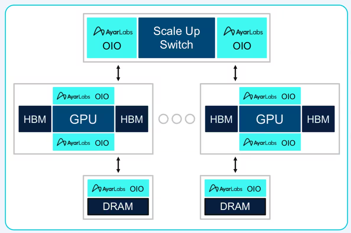
Scale-up first, extended memory next
The first commercial use of the technology will be for GPU scale-up architectures that connect accelerators within and across racks. “That’s the natural order of things,” says Stojanovic. “Optics is clearly becoming valuable for scale-up and multi-rack domains.”
The next step will be to link GPUs to extended memory (see diagram above). Using the same universal I/O chiplet, designers can partition bandwidth between inter-GPU communication and memory traffic depending on workload. “That lets you tailor performance efficiency — teraflops per watt — as well as interactivity [for inference],” he says.
The common element across both applications is flexibility: one optical die serving multiple system roles.
From racks to ‘islands’
Stojanovic expects that optical I/O will help expand the number of AI accelerators in a scale-up domain before scale-out becomes necessary.
“A single switch can’t have a radix much higher than about 512,” he explains. “With multi-die GPU packages, you can reach about 1,000 GPU dies per domain today, and in the next few years, we’ll see clusters of 1,000 to 10,000 GPU dies acting as one.”
He describes these as high-speed optical islands — units that operate as a single accelerator within a data-centre-scale cluster. “If you have 1,000,000 GPUs in a data centre, it’s a hundred islands of 10,000,” he says.
Optical I/O helps solve the key limitation of electrical networks: switch congestion. “In two-stage Clos networks, congestion is the problem. If you have plenty of bandwidth, you can enable path diversity — multiple switch planes — which dramatically reduces latency. An uncongested switch traversal is a few hundred nanoseconds.”
In effect, the bandwidth abundance that optical I/O delivers becomes a new lever for scaling compute clusters without compromising efficiency or latency.
Manufacturing and partnership
To bring the chip into high-volume manufacturing, Ayar has partnered with Alchip Technologies, a leading ASIC design house closely tied to TSMC. Alchip designs advanced ASICs and packages for hyperscalers and will integrate Ayar’s optical engines directly into compute or switch packages.
“When you make an optical engine, you need to put it in an advanced package — an xPU or switch package,” Stojanovic explains. “Alchip has the experience and market access in hyperscale. Together, we can provide a packaged ASIC decorated with optical engines that’s ready to connect at cluster scale.”
This arrangement, he adds, “helps hyperscalers de-risk deployment. The product is manufactured in a high-volume flow certified by TSMC, tested and qualified in that ecosystem.”
Ayar Labs is also partnering with a second leading Taiwanese ASIC player, Global Unichip Corp (GUC), to integrate its TeraPHY optical engine into GUC’s advanced ASIC design services. GUC is an ASIC processing and packaging company, with TSMC as its largest shareholder.
Competing to win
With multiple companies now targeting optical I/O, Stojanovic identifies three factors that will differentiate between the solutions.
“First is being in the right ecosystem — access to the best foundry and packaging partners,” he says. “Second is the form factor. It has to be manufacturable at scale; that’s why we chose chiplets.”
The third is maturity: proven reliability, validated system behaviour, and a roadmap that spans generations. “We’ve qualified our lasers, pushed our previous chips through reliability studies, and done thorough system-level validation. That’s what makes this technology ready for high-volume manufacturing.”
Will AI’s demand for GPUs and interconnect eventually slow? Stojanovic doubts it. “When people talk about slowing down, what that really means is slowing down for the end user,” he says. “Inside, you’re actually speeding up.”
Models may stabilise in size, but inference now chains multiple computations per query. “That means your one computation has to be ten times faster. Interactivity still matters,” he says.
Large clusters will therefore remain essential. “In the next two to five years, you’ll see between one and ten thousand GPU dies working as one in a cluster,” he predicts. “That’s the architecture optical I/O makes possible.”