
Next-generation coherent adds sub-carriers to capabilities
Part 2: Infinera's coherent toolkit
 Source: Infinera
Infinera has detailed coherent technology enhancements implemented using its latest-generation optical transmission technology. The system vendor is still to launch its newest photonic integrated circuit (PIC) and FlexCoherent DSP-ASIC but has detailed features the CMOS and indium phosphide ICs support.
The techniques highlight the increasing sophistication of coherent technology and an ever tighter coupling between electronics and photonics.
The company has demonstrated the technology, dubbed the Advanced Coherent Toolkit, on a Telstra 9,000km submarine link spanning the Pacific. In particular, the demonstration used matrix-enhanced polarisation-multiplexed, binary phased-shift keying (PM-BPSK) that enabled the 9,000km span without optical signal regeneration.
Using the ACT is expected to extend the capacity-reach product for links by the order of 60 percent. Indeed the latest coherent technology with transmitter-based digital signal processing delivers 25x the capacity-reach of 10-gigabit wavelengths using direct-detection, the company says.
Infinera’s latest PIC technology includes polarisation-multiplexed, 8-quadrature amplitude modulation (PM-8QAM) and PM-16QAM schemes. Its current 500-gigabit PIC supports PM-BPSK, PM-3QAM and PM-QPSK. The PIC is expected to support a 1.2-terabit super-channel and using PM-16QAM could deliver 2.4 terabit.
“This [the latest PIC] is beyond 500 gigabit,” confirms Pravin Mahajan, Infinera’s director of product and corporate marketing. “We are talking terabits now.”
Sterling Perrin, senior analyst at Heavy Reading, sees the Infinera announcement as less PIC related and more an indication of the expertise Infinera has been accumulating in areas such as digital signal processing.

Nyquist sub-carriers
Infinera is the first to announce the use of sub-carriers. Instead of modulating the data onto a single carrier, Infinera is using multiple Nyquist sub-carriers spread across a channel.
Using a flexible grid, the sub-carriers span a 37.5GHz-wide channel. In the example shown above, six are used although the number is variable depending on the link. The sub-carriers occupy 35GHz of the band while 2.5GHz is used as a guard band.
“Information you were carrying across one carrier can now be carried over multiple sub-carriers,” says Mahajan. “The benefit is that you can drive this as a lower-baud rate.”
Lowering the baud rate increases the tolerance to non-linear channel impairments experienced during optical transmission. “The electronic compensation is also much less than what you would be doing at a much higher baud rate,” says Abhijit Chitambar, Infinera’s principal product and technology marketing manager.
While the industry is looking to increase overall baud rate to increase capacity carried and reduce cost, the introduction of sub-carriers benefits overall link performance. “You end up with a better Q value,” says Mahajan. The ‘Q’ refers to the Quality Factor, a measure of the transmission’s performance. The Q Factor combines the optical signal-to-noise ratio (OSNR) and the optical bandwidth of the photo-detector, providing a more practical performance measure, says Infinera.
Infinera has not detailed how it implements the sub-carriers. But it appears to be a combination of the transmitter PIC and the digital-to-analogue converter of the coherent DSP-ASIC.
It is not clear what the hardware implications of adopting sub-carriers are and whether the overall DSP processing is reduced, lowering the ASIC’s power consumption. But using sub-carriers promotes parallel processing and that promises chip architectural benefits.
“Without this [sub-carrier] approach you are talking about upping baud rate,” says Mahajan. “We are not going to stop increasing the baud rate, it is more a question of how much you can squeeze with what is available today.“
SD-FEC enhancements
The FlexCoherent DSP also supports enhanced soft-decision forward-error correction (SD-FEC) including the processing of two channels that need not be contiguous.
SD-FEC delivers enhanced performance compared to conventional hard-decision FEC. Hard-decision FEC decides whether a received bit is a 1 or a 0; SD-FEC also uses a confidence measure as to the likelihood of the bit being a 1 or 0. This additional information results in a net coding gain of 2dB compared to hard-decision FEC, benefiting reach and extending the life of submarine links.
By pairing two channels, Infinera shares the FEC codes. By pairing a strong channel with a weak one and sharing the codes, some of the strength of the strong signal can be traded to bolster the weaker one, extending its reach or even allowing for a more advanced modulation scheme to be used.
The SD-FEC can also trade performance with latency. SD-FEC uses as much as a 35 percent overhead and this adds to latency. Trading the two supports those routes where low latency is a priority.
Matrix-enhanced PSK
Infinera has implemented a technique that enhances the performance of PM-BPSK used for the longest transmission distances such as sub-sea links. The matrix-enhancement uses a form of averaging that adds about a decibel of gain. “Any innovation that adds gain to a link, the margin that you give to operators is always welcome,” says Mahajan.
The toolkit also supports the fine-tuning of channel widths. This fine-tuning allows the channel spacing to be tailored for a given link as well as better accommodating the Nyquist sub-carriers.
Product launch
The company has not said when it will launch its terabit PIC and FlexCoherent DSP.
“Infinera is saying it is the first announcing Nyquist sub-carriers, which is true, but they don’t give a roadmap when the product is coming out,” says Heavy Reading’s Perrin. “I suspect that Nokia [Alcatel-Lucent], Ciena and Huawei are all innovating on the same lines.”
There could be a slew of announcements around the time of the OFC show in March, says Perrin: “So Infinera could be first to announce but not necessarily first to market.”
AppliedMicro samples 100Gbps CMOS multiplexer
AppliedMicro has announced the first CMOS merchant multiplexer chip for 100Gbps coherent optical transmission. The S28032 device supports dual polarisation, quadrature phase-shift keying (DP-QPSK) and has a power consumption of 4W, half that of current multiplexer chip designs implemented in BiCMOS.
 The S28032 100 Gig multiplexer IC. Source: AppliedMicro
"CMOS has a very low gain-bandwidth product, typically 100GHz," says Tim Warland, product marketing manager, connectivity solutions at AppliedMicro. “Running at 32GHz, we have been able to achieve a very high bandwidth with CMOS."
Significance
The availability of a CMOS merchant device will be welcome news for optical transport suppliers and 100Gbps coherent module makers. CMOS has better economics than BiCMOS due to the larger silicon wafers used and the chip yields achieved. The reduced power consumption also promotes the move to smaller-sized optical modules than the current 5x7-inch multi-source agreement (MSA).
"By reducing the power and the size, we can get to a 4x6-inch next-generation module,” says Warland. “And perhaps if we go for a shorter [optical transmission] reach - 400-600km - we could get into a CFP; then you can get four modules on a card.”
"Coherent ultimately is the solution people want to go to [in the metro] but optical duo-binary will do just fine for now"
Tim Warland, AppliedMicro
Chip details
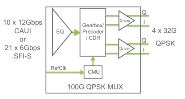
The S28032 has a CAUI interface: 10x12Gbps input lanes that are multiplexed into four lanes at 28Gbps to 32Gbps. The particular data rate depends on the forward error correction (FEC) scheme used. The four lanes are DQPSK-precoded before being fed to the polarisation multiplexer to create the DP-QPSK waveforms.
The device also supports the SFI-S interface - 21 input channels, each at 6Gbps. This is significant as it enables the S28032 to be interfaced to NTT Electronics' (NEL) DSP-ASIC coherent receiver chip that has been adopted by 100Gbps module makers Oclaro and Opnext (now merged) as well as system vendors including Fujitsu Optical Systems and NEC.
 The mux IC within a 100Gbps coherent 5x7-inch optical module. Source: AppliedMicro
The AppliedMicro multiplexer IC, which is on the transmit path, interfaces with NEL's DSP-ASIC that is on the receiver path, because the FEC needs to be a closed loop to achieve the best efficiency, says Warland. "If you know what you are transmitting and receiving, you can improve the gain and modify the coherent receiver sampling points if you know what the transmit path looks like," he says.
The DSP-ASIC creates the transmission payloads and uses the S28032 to multiplex those into 28Gbps or greater speed signals.
The SFI-S interface is also suited to interface to FPGAs, for those system vendors that have their own custom FPGA-based FEC designs.
"Packet optical transport systems is more a potential growth engine as the OTN network evolves to become a real network like SONET used to be"
Francesco Caggioni. AppliedMicro
The multiplexer chip's particular lane rate is set by the strength of the FEC code used and its associated overhead. Using OTU4 frames with its 7% overhead FEC, the resulting data rate is 27.95Gbps. With a stronger 15% hard-decision FEC, each of the 4 channel's data rate is 30Gbps while it is 31.79Gbps with soft-decision FEC.
"It [the chip] has got sufficient headroom to accommodate everything that is available today and that we are considering in the OIF [Optical Internetworking Forum],” says Warland. The multiplexer is expected to be suitable for coherent designs that achieve a reach of up to 2,000-2,500km but the sweet spot is likely to be for metro networks with a reach of up to 1,000km, he says.
But while the CMOS device can achieve 32Gbps, it has its limitations. "For ultra long haul, we can't support a FEC rate higher than 20%," says Warland. "For that, a 25% to 30% FEC is needed."
AppliedMicro is sampling the device to lead customers and will start production in 1Q 2013.
What next
The S28032 joins AppliedMicro's existing S28010 IC suited for the 10km 100 Gigabit Ethernet 100GBASE-LR4 standard, and for optical duo-binary 100Gbps direct detection that has a reach of 200-1,000km.
"Our next step is to try and get a receiver to match this chip," says Warland. But it will be different to NEL's coherent receiver: "NEL's is long haul." Instead, AppliedMicro is eyeing the metro market where a smaller, less power-hungry chip is needed.
"Coherent ultimately is the solution people want to go to [in the metro] but optical duo-binary will do just fine for now," says Warland.
Two million 10Gbps OTN ports
AppliedMicro has also announced that it has shipped 2M 10Gbps OTN silicon ports. This comes 18 months after it announced that it had shipped its first million.
"OTN is showing similar growth to the 10 Gigabit Ethernet market but with a four-year lag," says Francesco Caggioni, strategic marketing director, connectivity solutions at AppliedMicro.
The company sees OTN growth in the IP edge router market and for transponder and muxponder designs, while packet optical transport systems (P-OTS) is an emerging market.
"Packet optical transport systems is more a potential growth engine as the OTN network evolves to become a real network like SONET used to be," says Caggioni. "We are seeing development but not a lot of deployment."
Further reading:
How ClariPhy aims to win over the system vendors

“We can build 200 million logic gate designs”
Reza Norouzian, ClariPhy
ClariPhy is in the camp that believes that the 100 Gigabit-per-second (Gbps) market is developing faster than people first thought. “What that means is that instead of it [100Gbps] being deployed in large volumes in 2015, it might be 2014,” says Reza Norouzian, vice president of worldwide sales and business development at ClariPhy.
Yet the fabless chip company is also glad it offers a 40Gbps coherent IC as this market continues to ramp while 100Gbps matures and overcomes hurdles common to new technology: The 100Gbps industry has yet to develop a cost-effective solution or a stable component supply that will scale with demand.
Another challenge facing the industry is reducing the power consumption of 100Gbps systems, says Norouzian. The need to remove the heat from a 100Gbp design - the ASIC and other components - is limiting the equipment port density achievable. “If you require three slots to do 100 Gig - whereas before you could use these slots to do 20 or 30, 10 Gig lines - you are not achieving the density and economies of scale hoped for,” says Norouzian.
40G and 100G coherent ASICs
ClariPhy has chosen a 40nm CMOS process to implement its 40Gbps coherent chip, the CL4010. But it has since decided to adopt 28nm CMOS for its 100Gbps design – the CL10010 - to integrate features such as soft-decision forward error correction (see New Electronics' article on SD-FEC) and reduce the chip’s power dissipation.
The CL4010 integrates analogue-to-digital and digital-to-analogue converters, a digital signal processor (DSP) and a multiplexer/ demultiplexer on-chip. “Normally the mux is a separate chip and we have integrated that,” says Norouzian.
The first CL4010 samples were delivered to select customers three months ago and the company expects volume production to start by the end of September. The CL4010 also interoperates with Cortina Systems’ optical transport network (OTN) processor family of devices, says the company.
The start-up claims there is strong demand for the CL4010. “When we ask them [operators]: ‘With all the hoopla about 100 Gig, why are you buying all this 40 Gig?’, the answer is that it is a pragmatic solution and one they can ship today,” says Norouzian.
ClariPhy expects 40Gbps volumes to continue to ramp for the next three or four years, partly because of the current high power consumption of 100Gbps. The company says several system vendors are using the CL4010 in addition to optical module customers.
The 28nm 100Gbps CL10010 is a 100 million gate ASIC. ClariPhy acknowledges it will not be first to market with an 100Gbps ASIC but that by using the latest CMOS process it will be well position once volume deployments start from 2014.
ClariPhy is already producing a quad-10Gbps chip implementing the maximum likelihood sequence estimation (MLSE) algorithm used for dispersion compensation in enterprise applications. The device covers links up to 80km (10GBASE-ZR) but the main focus is for 10GBASE-LRM (220m+) applications. “Line cards that used to have four times 10Gbps lanes now are moving to 24 and will use six of these chips,” says Norouzian. The device sits on the card and interfaces with SFP+ or Quad-SFP optical modules.
“The CL10010 is the platform to demonstrate all that we can do but some customers [with IP] will get their own derivatives”
System vendor design wins
The 100Gbps transmission ASIC market may be in its infancy but the market is already highly competitive with clear supply lines to the system vendors.
Several leading system vendors have decided to develop their own ASICs. Alcatel-Lucent, Ciena, Cisco Systems (with the acquisition of CoreOptics), Huawei and Infinera all have in-house 100Gbps ASIC designs.
System vendors have justified the high development cost of the ASIC to get a time-to-market advantage rather than wait for 100Gbps optical modules to become available. Norouzian also says such internally-developed 100Gbps line card designs deliver a higher 100Gbps port density when compared to a module-based card.
Alternatively, system vendors can wait for 100Gbps optical modules to become available from the likes of an Oclaro or an Opnext. Such modules may include merchant silicon from the likes of a ClariPhy or may be internally developed, as with Opnext.
System vendors may also buy 100Gbps merchant silicon directly for their own 100Gbps line card designs. Several merchant chip vendors are targeting the coherent marketplace in addition to ClariPhy. These include such players as MultiPhy and PMC-Sierra while other firms are known to be developing silicon.
Given such merchant IC competition and the fact that leading system vendors have in-house designs, is the 100Gbps opportunity already limited for ClariPhy?
Norouzian's response is that the company, unlike its competitors, has already supplied 40Gbps coherent chips, proving the company’s mixed signal and DSP expertise. The CL10010 chip is also the first publicly announced 28nm design, he says: “Our standard product will leapfrog first generation and maybe even second generation [100Gbps] system vendor designs.”
The equipment makers' management will have to decide whether to fund the development of their own second-generation ASICs or consider using ClariPhy’s 28nm design.
ClariPhy acknowledges that leading system vendors have their own core 100Gbps intellectual property (IP) and so offers vendors a design service to develop their own custom systems-on-chip. For example a system vendor could use ClariPhy's design but replace the DSP core with the system vendor’s own hardware block and software.
 Source: ClariPhy Communications
Norouzian says system vendors making 100Gbps ASICs develop their own intellectual property (IP) blocks and algorithms and use companies like IBM or Fujitsu to make the design. ClariPhy offers a similar service while also being able to offer its own 100Gbps IP as required. “The CL10010 is the platform to demonstrate all that we can do,” says Norouzian. “But some customers [with IP] will get their own derivatives.”
The firm has already made such custom coherent devices using customers’ IP but will not say whether these were 40 or 100Gbps designs.
Market view
ClariPhy claims operator interest in 40Gbps coherent is not so much because of its superior reach but its flexibility when deployed in networks alongside existing 10Gbps wavelengths. “You don't have to worry about [dispersion] compensation along routes,” says Norouzian, adding that coherent technology simplifies deployments in the metro as well as regional links.
And while ClariPhy’s focus is on coherent systems, the company agrees with other 100Gbps chip specialists such as MultiPhy for the need for 100Gbps direct-detect solutions for distances beyond 40km. “It is very likely that we will do something like that if the market demand was there,” says Norouzian. But for now ClariPhy views mid-range 100Gbps applications as a niche opportunity.
Funding
ClariPhy raised US $14 million in June. The biggest investor in this latest round was Nokia Siemens Networks (NSN).
An NSN spokesperson says working with ClariPhy will help the system vendor develop technology beyond 100Gbps. “It also gives us a clear competitive edge in the optical network markets, because ClariPhy’s coherent IC and technology portfolio will enable us to offer differentiated and scalable products,” says the spokesperson.
The funding follows a previous round of $24 million in May 2010 where the investors included Oclaro. ClariPhy has a long working relationship with the optical components company that started with Bookham, which formed Oclaro after it merged with Avanex.
“At 100Gbps, Oclaro get some amount of exclusivity as a module supplier but there is another module supplier that also gets access to this solution,” says Norouzian. This second module supplier has worked with ClariPhy in developing the design.
ClariPhy will also supply the CL10010 to the system vendors. “There are no limitations for us to work with OEMs,” he says.
The latest investment will be used to fund the company's R&D effort in 100, 200 and 400Gbps, and getting the CL4010 to production.
Beyond 100 Gig
The challenge at higher data rates that 100Gbps is implementing ultra-large ASICs: closing the timings and laying out vast digital circuitry. This is an area the company has been investing in over the last 18 months. “Now we can build 200 million logic gate designs,” says Norouzian.
Moving from 100Gbps to 200Gbps wavelengths will require higher order modulation, says Norouzian, and this is within the realm of its ASIC.
Going to 400Gbps will require using two devices in parallel. One Terabit transmission however will be far harder. “Going to one Terabit requires a whole new decade of development,” he says.
Further reading: