
Q&A with Rafik Ward - Part 1
 "This is probably the strongest growth we have seen since the last bubble of 1999-2000." Rafik Ward, Finisar
Q: How would you summarise the current state of the industry?
A: It’s a pretty fun time to be in the optical component business, and it’s some time since we last said that.
We are at an interesting inflexion point. In the past few years there has been a lot of emphasis on the migration from 1 to 2.5 Gig to 10 Gig. The [pluggable module] form factors for these speeds have been known, and involved executing on SFP, SFP+ and XFPs.
But in the last year there has been a significant breakthrough; now a lot of the discussion with customers are around 40 and 100 Gig, around form factors like QSFP and CFP - new form factors we haven’t discussed before, around new ways to handle data traffic at these data rates, and new schemes like coherent modulation.
It’s a very exciting time. Every new jump is challenging but this jump is particularly challenging in terms of what it takes to develop some of these modules.
From a business perspective, certainly at Finisar, this is probably the strongest growth we have seen since the last bubble of 1999-2000. It’s not equal to what it was then and I don’t think any of us believes it will be. But certainly the last five quarters has been the strongest growth we’ve seen in a decade.
What is this growth due to?
There are several factors.
There was a significant reduction in spending at the end of 2008 and part of 2009 where end users did not keep up with their networking demands. Due to the global financial crisis, they [service providers] significantly cut capex so some catch-up has been occurring. Keep in mind that during the global financial crisis, based on every metric we’ve seen, the rate of bandwidth growth has been unfazed.
From a Finisar perspective, we are well positioned in several markets. The WSS [wavelength-selective switch] ROADM market has been growing at a steady clip while other markets are growing quite significantly – at 10 Gig, 40 Gig and even now 100 Gig. The last point is that, based on all the metrics we’ve seen, we are picking up market share.
Your job title is very clear but can you explain what you do?
I love my job because no two days are the same. I come in and have certain things I expect to happen and get done yet it rarely shapes out how I envisaged it.
There are really three elements to my job. Product management is the significant majority of where I focus my efforts. It’s a broad role – we are very focussed on the products and on the core business to win market share. There is a pretty heavy execution focus in product management but there is also a strategic element as well.
The second element of my job is what we call strategic marketing. We spend time understanding new, potential markets where we as Finisar can use our core competencies, and a lot of the things we’ve built, to go after. This is not in line with existing markets but adjacent ones: Are there opportunities for optical transceivers in things like military and consumer applications?
One of the things I’m convinced of is that, as the price of optical components continues to come down, new markets will emerge. Some of those markets we may not even know today, and that is what we are finding. That’s a pretty interesting part of my job but candidly I spend quite a bit less time on it [strategic marketing] than product management.
The third area is corporate communications: talking to media and analysts, press releases, the website and blog, and trade shows.
"40Gbps DPSK and DQPSK compete with each other, while for 40 Gig coherent its biggest competitor isn’t DPSK and DQPSK but 100 Gig."
Some questions on markets and technology developments.
Is it becoming clearer how the various 40Gbps line side optics – DPSK, DQPSK and coherent – are going to play out?
The situation is becoming clearer but that doesn’t mean it is easier to explain.
The market is composed of customers and end users that will use all of the above modulation formats. When we talk to customers, every one has picked one, two or sometimes all three modulation formats. It is very hard to point to any trend in terms of picks, it is more on a case-by-case basis. Customers are, like us at the component level, very passionate about the modulation format that they have chosen and will have a variety of very good reasons why a particular modulation format makes sense.
Unlike certain markets where you see a level of convergence, I don’t think that there will be true convergence at 40 Gbps. Coherent – DP-QPSK - is a very powerful technology but the biggest challenge 40 Gig has with DP-QPSK is that you have the same modulation format at 100 Gig.
The more I look at the market, 40Gbps DPSK and DQPSK compete with each other, while for 40 Gig coherent its biggest competitor isn’t DPSK and DQPSK but 100 Gig.
Finisar has been quiet about its 100 Gig line side plans, what is its position?
We view these markets - 40 and 100 Gig line side – as potentially very large markets at the optical component level. Despite that fact that there are some customers that are doing vertical integrated solutions, we still see these markets as large ones. It would be foolish for us not to look at these markets very carefully. That is probably all I would say on the topic right now.
"Photonic integration is important and it becomes even more important as data rates increase."
Finisar has come out with an ‘optical engine’, a [240Gbps] parallel optics product. Why now?
This is a very exciting part of our business. We’ve been looking for some time at the future challenges we expect to see in networking equipment. If you look at fibre optics today, they are used on the front panel of equipment. Typically it is pluggable optics, sometimes it is fixed, but the intent is that the optics is the interface that brings data into and out of a chassis.
People have been using parallel optics within chassis – for backplane and other applications – but it has been niche. The reason it’s niche is that the need hasn’t been compelling for intra-chassis applications. We believe that need will change in the next decade. Parallel optics intra-chassis will be needed just to be able to drive the amount of bandwidth required from one printed circuit board to another or even from one chip to another.
The applications driving this right now are the very largest supercomputers and the very largest core routers. So it is a market focussed on the extreme high-end but what is the extreme high-end today will be mainstream a few years from now. You will see these things in mainstream servers, routers and switches etc.
Photonic integration – what’s happening here?
Photonic integration is something that the industry has been working on for several years in different forms; it continues to chug on in the background but that is not to understate its importance.
For vendors like Finisar, photonic integration is important and it becomes even more important as data rates increase. What we are seeing is that a lot of emerging standards are based around multiple lasers within a module. Examples are the 40GBASE-LR4 and the 100GBASE-LR4 (10km reach) standards, where you need four lasers and four photo-detectors and the corresponding mux-demux optics to make that work.
The higher the number of lasers required inside a given module, and the more complexity you see, the more room you have to cost-reduce with photonic integration.
Bringing WDM-PON to market

"We see just one way to bring down the cost, form-factor and energy consumption of the OLT’s multiple transceivers: high integration of transceiver arrays"
Klaus Grobe, ADVA Optical Networking
Considerable engineering effort will be needed to make next-generation optical access schemes using multiple wavelengths competitive with existing passive optical networks (PONs).
Such a multi-wavelength access scheme, known as a wavelength division multiplexing-passive optical network (WDM-PON), will need to embrace new architectures based on laser arrays and reflective optics, and use advanced photonic integration to meet the required size, power consumption and cost targets.
Current PON technology uses a single wavelength to deliver downstream traffic to end users. A separate wavelength is used for upstream data, with each user having an assigned time slot to transmit.
Gigabit PON (GPON) delivers 2.5 Gigabit-per-second (Gbps) to between 32 or 64 users, while the next development, XG-PON, will extend GPON’s downstream data rate to 10 Gbps. The alternative PON scheme, Ethernet PON (EPON), already has a 10 Gbps variant. Vendors are also extending PON’s reach from 20km to 80km or more using signal amplification.
But the industry view is that after 10 Gigabit PON, the next step will be to introduce multiple wavelengths to extend the capacity beyond what a time-sharing approach can support. Extending the access network's reach to 100km will also be straightforward using WDM transport technology.
The advent of WDM-PON is also an opportunity for new entrants, traditional WDM optical transport vendors, to enter the access market. ADVA Optical Networking is one firm that has been vocal about its plans to develop next-generation access systems.
“We are seriously investigating and developing a next-generation access system and it is very likely that it will be a flavour of WDM-PON,” says Klaus Grobe, senior principal engineer at ADVA Optical Networking. “It [next-generation access] must be based on WDM simply because of bandwidth requirements.”
The system vendor views WDM-PON as addressing three main applications: wireless backhaul, enterprise connectivity and residential broadband. But despite WDM-PON’s potential to reduce operating costs significantly, the challenge facing vendors is reducing the cost of WDM-PON hardware. Indeed it is the expense of WDM-PON systems that so far has assigned the technology to specialist applications only.
 A non-reflective tunable laser-based WDM-PON ONU. Source: ADVA Optical NetworkingAccording to Grobe, cost reduction is needed at both ends of the WDM-PON: the client receiver equipment known as the optical networking unit (ONU) and the optical line terminal (OLT) housed within an operator’s central office.
ADVA Optical Networking plans to use low-cost tunable lasers rather than a broadband light source and reflective optics for the ONU transceivers. “For the OLT, we see just one way to bring down the cost, form-factor and energy consumption of the OLT’s multiple transceivers: high integration of transceiver arrays,” says Grobe.
This is a considerable photonic integration challenge: a 40- or 80-wavelength WDM-PON uses 40 or 80 transceiver bi-directional clients, equating to 80 and 160 wavelengths. If 80 SFPs optical modules were used at the OLT, the resulting cost, size and power consumption would be prohibitive, says Grobe.
ADVA Optical Networking is working with several firms, one being CIP Technologies, to develop integrated transceiver arrays. ADVA Optical Networking and CIP Technologies are part of the EU-funded project, C-3PO, that includes the development of integrated transceiver arrays for WDM-PON.
Splitters versus filters
One issue with WDM-PON is that there is no industry-accepted definition. ADVA Optical Networking views WDM-PON as an architecture based on optical filters rather than splitters. Two consequences result once that choice is made, says Grobe.
One is insertion loss. Choosing filters implies arrayed waveguide gratings (AWGs), says Grobe. “No other filter technology is seriously considered for WDM-PON if filters are used,” he says.
With an AWG, the insertion loss is independent of the number of wavelengths supported. This differs from using a splitter-based architecture where every 1x2 device introduces a 3dB loss - “closer to 3.5dB”, he says. Using a 1x64 splitter, the insertion loss is 14 or 15dB whereas for a 40-channel AWG the loss can be as low as 4dB. “I just saw specs of a first 96-channel AWG, even that one isn’t much higher [than 4dB],” says Grobe. Thus using filters rather than splitters, the insertion loss is much lower for a comparable number of client ONUs.
There is also a cost benefit associated with a low insertion loss. To limit the cost of next-generation PON, the transceiver design must be constrained to a 25dB power budget associated with existing PON transceivers. “This is necessary to keep these things cheap, possibly dirt cheap,” says Grobe.
The alternative, using XG-PON’s sophisticated 10 Gbps burst-mode transceiver with its associated 35dB power budget, achieving low cost is simply not possible, he says. To live with transceivers with a 25dB power budget, the insertion loss of the passive distribution network must be minimised, explaining why filters are favoured.
The other main benefit of using filters is security. With a filter-based PON, wavelength point-to-point connections result. “You are not doing broadcast,” says Grobe. “You immediately get rid of almost all security aspects.” This is an issue with PON where traffic is shared.
Low power
Achieving a low-power WDM-PON system is another key design consideration. “In next-gen access, it is absolutely vital,” says Grobe. “If the technology is deployed on a broad scale - that is millions of user lines – every single watt counts, otherwise you end up with differences in the approaches that go into the megawatts and even gigawatts.”
There is also a benchmarking issue, says Grobe: the WDM-PON OLT will be compared to XG-PON’s even if the two schemes differ. Since XG-PON uses time-division multiplexing, there will be only one transceiver at the OLT. But this is what a 40- or 80-channel WDM-PON OLT will be compared with, even if the comparison is apples to pears, says Grobe.
WDM-PON workings
There are two approaches to WDM-PON.
In a fully reflective architecture, the OLT array and the ONUs are seeded using multi-wavelength laser arrays; both ends use the lasers arrays in combination with reflective optics for optical transmission.
ADVA Optical Networking is interested in using a reflective approach at the OLT but for the ONU it will use tunable lasers due to technical advantages. For example, using the same wavelength for the incoming and modulated streams in a reflective approach, Rayleigh crosstalk is an issue when the ONUs are 100km from the OLT. In contrast, Rayleigh crosstalk at the OLT is avoided because the multi-wavelength laser array is located only a few metres from the reflective electro-absorption modulators (REAMs).
REAMs are used rather than semiconductor optical amplifiers (SOAs) to modulate data at the OLT because they support higher bandwidth 10 Gbps wavelengths. Indeed the C-3PO project is likely to use a monolithically integrated SOA-REAM for this task. “The reflective SOA is narrower in bandwidth but has inherent gain while the REAM has loss rather than gain – it is just a modulator,” says Grobe. “The combination of the two is the ideal: giving high modulation bandwidth and high transmit power.”
 The integrated WDM-PON OLT. In practice the transmit array uses a reflective architecture based on SOA-REAMs and is fed with a multi-wavelength laser source. Source: ADVA Optical Networking
For the OLT, a multi-wavelength laser is fed via an AWG into an array of SOA-REAMs which modulate the wavelengths and return them through the AWG where they are multiplexed and transmitted to the ONUs via a demultiplexing AWG. An added benefit of this approach, says Grobe, is that the same multi-wavelength laser source can be use to feed several WDM-PON OLTs, further decreasing system cost.
For the upstream path, each ONU’s wavelength is separated by the OLT’s AWG and fed to the receiver array. In a WDM-PON system, the OLT transmit wavelengths and receive wavelengths (from the ONUs) operate in separate optical bands.
Grobe expects its resulting WDM-PON system to use 40 or 80 channels. And to best meet size, power and cost constraints, the OLT design will likely implemented as a photonic integrated circuit. “We are after a single PIC solution,” he says. “It is clear that with the OLT, integration is the only way to meet requirements.” A photonically-integrated OLT design is one of the products expected from the C-3PO project, using CIP Technologies' hybrid integration technology.
ADVA Optical Networking has already said that its WDM-PON OLT will be implemented using its FSP 3000 platform.
- To see some WDM-PON architecture slides, click here.
UNIC silicon modulator
This is the silicon photonic start-up’s first announced modulator. The design has been developed in conjunction with Sun Microsystems as part of the DAPRA Ultraperformance Nanophotonic Intrachip Communications (UNIC) programme.
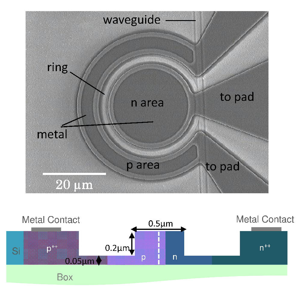 An image of the modulator and a cross-section diagram of the ring waveguide. Source: Kotura
Why is it important?
Optical components use a range of specialist, expensive materials. Silicon is one material that could transform the economics for optics. But for this to happen, the main optical functions – light generation, transmission and detection – need to be supported in silicon. To date, all the required functions except the laser itself - waveguides, modulators and photo-detectors - have been mastered and implemented in silicon.
However, the use of silicon photonics in commercial products has till now been limited. For example, Luxtera makes active optical cable that uses silicon photonics-based transceivers while Kotura has been producing silicon photonics-based VOAs for several years. Its VOA is used within reconfigurable optical add/drop multiplexers (ROADMs) and as a dimmer switch to protect optical receivers from network transients.
Kotura is also supplying its silicon-based Echelle gratings product for 40 and 100 Gigabit Ethernet (GbE) transceiver designs that require the multiplexing and demultiplexing of 4 and 10 wavelengths. The company’s gratings are also being used in Santur’s 100Gbit/s (10x10Gbit/s) transceiver design.
Kotura is in volume production of its VOAs and sampling its Ethernet gratings products, says Arlon Martin, vice-president of marketing and sales at Kotura: “The biggest interest is in 40 Gigabit Ethernet.” Given the small size of the gratings, Kotura is also seeing interest from vendors developing 40GbE transceivers in smaller form factors than the CFP module, such as the QSFP.
This will enable 1Tbit/s data rates over a single fibre to connect high-speed multi-core processor computing elements.
Arlon Martin of Kotura.
But the true potential for silicon photonics, one that promises huge volumes, is very short reach optical interconnects for use in high performance computing and within data centres. Having a low power silicon modulator means it can be integrated with other circuitry in CMOS rather than as a discrete design. Such an integrated approach ensures interconnect reliability.
Method used
There are several ways to modulate a laser. Direct modulation uses electronics to switch the laser on and off at the required rate to imprint the data onto the light. An electro-absorption modulated laser, in contrast, adds an element in front of an always-on laser that either passes or absorbs the light. Kotura’s modulator uses a third approach based on a micro-ring resonator and an adjacent waveguide.
The dimension of the ring – its circumference – dictates when optical resonance occurs. And by carefully matching the power coupling of the micro-ring and waveguide to that of the ring loss, signal attenuation– the light-off condition – is improved. The wavelength at which resonance occurs can be changed by playing with the optical properties of the ring waveguide.
Kotura and Sun have demonstrated the silicon modulator working at up to 11GHz, requiring a peak-to-peak voltage of 2V only. The modulator’s insertion loss is also an attractive 2dB though its working spectrum width is only 0.1nm.
“Our power number – 0.5mW at 10GHz - does not include the driver. But if you want to integrate a number of these on one chip, the low power consumption would enable this,” says Martin. Kotura claims the power consumption achieved is the lowest yet reported.
What next?
The modulator is one of the milestones of the DARPA UNIC programme now into the second of its five-year duration. “This [modulator] is prototype work, not a product,” says Martin, adding that Kotura has not fixed a date as to when the modulator will be commercially used.
As for how the device will ultimately be used, Kotura talks of interfaces operating between 100Gbit/s and 1 Tbit/s. Kotura is already working on an independent programme with CyOptics - the NIST Advanced Technology Programme - developing up to 1Tbit/s links using wavelength division multiplexing (WDM). Such designs use separate laser arrays - each laser at a specific wavelength – as well as gratings and photo-detectors.
In the future inexpensive light sources could generate up to 80 separate modulated lightpaths, Martin says. This will enable 1Tbit/s data rates over a single fibre to connect high-speed multi-core processor computing elements.
Is the idea similar to a broadband light source as proposed for WDM-PON? The UNIC partners have yet to reveal the programme’s detail. “Potentially on the right path,” is all Martin would say.
References:
[1] “Low Vpp, ultralow-energy, compact, high-speed silicon electro-optic modulator.” To read Kotura’s technical paper, click here.
[2] "PHOTONICS APPLIED: INTEGRATED PHOTONICS: Can optical integration solve the computational bottleneck?" OptoIQ, March 1, 2009, click here.
Mind maps

To download the full mind map in .pdf form, click here.

Photonic integration: Bent on disruption
“This is a general rule: what starts as a series of parts loosely strung together, if used heavily enough, congeals into a self-contained unit.”
W. Brian Arthur, The Nature of Technology
 Infinera's Dave Welch: PICs are fibre-optic's current disruption
Dave Welch likes to draw a parallel with digital photography when discussing the use of photonic integration for optical networking. “The CMOS photodiode array – a photonic integrated circuit - changed the entire supply chain of photography,” says Welch, the chief strategy officer at Infinera.
Applied to networking, the photonic integrated circuit (PIC) is similar, argues Welch. It benefits system cost by integrating individual optical components but it delivers more. “All the value – inherently harder to pin down - of networking efficiency of a system that isn’t transponder-based,” says Welch.
Just how disruptive a technology the PIC proves to be is unclear but there is no doubting the growing role of optical integration.
“Integration is a key part of our thinking,” says Sam Bucci, vice president, WDM, Alcatel-Lucent’s optics activities. When designing a new platform, Alcatel-Lucent surveys components and techniques to identify disruptive technologies. Even if it chooses to implement functions using discrete components, the system is designed taking into account future integrated implementations.
“We are seeing interest [in photonic integration] across the spectrum," says Stefan Rochus, vice president of marketing and business development at CyOptics. "Long-haul, metro, access and chip-to-chip - everything is in play."
The drivers for optical integration’s greater use are harder to pin down.
Operators must contend with yearly data traffic growth estimated at between 45 to 65 percent yet their revenues are growing modestly. “It’s no secret that the capacity curve - whether the line side or the client side - is growing at an astonishing clip,” says Bucci.
The onus is thus on equipment and component makers to deliver platforms that reduce the transport cost per bit."Delivering more for less," says Graeme Maxwell, vice president of hybrid integration at CIP Technologies. “Space is a premium, power is an issue, operators want performance maintained or improved – all are driving integration.”
Cost is an issue for optical components with yearly price drops of 20 percent being common. “Hitting the cost-curve, we have run out of ways to do that with classic optics,” says Sinclair Vass, commercial director, EMEA at JDS Uniphase.
High-speed optical transmission at 40 and 100 Gigabit per second (Gbps) requires photonic integration though here the issues are as much performance as cost reduction. Indeed, its use can be viewed as the result of the integration between electronics and optics. To address optical signal impairments, chips must work at the edge of their performance, requiring the optical signal to be split into slower, parallel streams. Such an arrangement is ripe for photonic integration.
“It is as if there are two kinds of integration: at the boundary between optics and electronics, and the purely optical planar waveguide stuff,” says Karen Liu, vice president, components and video technologies at market research firm Ovum.
The other market where the full arsenal of optical integration techniques – hybrid and monolithic integration – is being applied is optical transceivers for passive optical networking (PON). Here the sole story is cost.
As old as the integrated circuit
Photonic integration is not new. The idea was first mooted in a 1969 AT&T Bell Labs’ paper that described how multiple miniature optical components could be interconnected via optical waveguides made using thin-film dielectric materials. But so far industry adoption for optical networking has been limited.

"Two kinds of integration: at the boundary between optics and electronics, and the purely optical planar waveguide stuff"
Karen Liu, Ovum
Heavy Reading, in a 2008 report, highlighted the limited progress made in photonic integration in recent years, with the exception of Infinera, a maker of systems based on a dense wavelength division multiplexing (DWDM) 10x10Gbps monolithically integrated PIC.
“Infinera has held very consistently to its original story, including sub-wavelength grooming, and have made progress over time,” says Liu. But she points out a real disruptive impact has not yet been seen: “The problem with the digital camera analogy is that something that is disruptive is not a straight replacement but implies the next step: changing the network architecture, not just how a system is implemented.”
On-off keying to phase modulation
One way operators are accommodating traffic growth is cramming more data down a fibre. It is this trend- from 10Gbps to 40 and 100Gbps lightpaths - that is spurring photonic integration.
“If you look at current 100 Gigabit, it is a bigger configuration than we would like,” says Joe Berthold, Ciena’s vice president of network architecture. Ciena’s first 100Gbps design requires three line cards, taking five inches of rack space, while its second-generation design will fit on a single, two-inch card.
Both 40 and 100Gbps transmissions must also operate over existing networks, matching the optical link performance of 10Gbps despite dispersion being more acute at higher line speeds. To meet the challenge, the industry has changed how it modulates data onto light. Whereas previous speed increments up to 10Gbps used simple on-off keying, 40 and 100Gbps use advanced modulation schemes based on phase, or phase combined with polarisation.
The modulation schemes split the optical signal into parallel paths to lower symbol rates. For example, 40Gbps differential quadrature phase-shift keying (DQPSK) uses two signals that effectively operating at 20 Gigabaud. Halving the rate relaxes the high-speed electronics requirements at the expense of complicating the optical circuitry.
The concept is extended further at 100Gbps. Here polarisation is combined with phase modulation (either DQPSK, or QPSK if coherent detection is used) such that four signals are used in parallel, each operating at 28 Gigabaud.

“The 40/100G area is shaping up to be the equivalent of breaking the sound barrier”
Brad Smith, LightCounting
“Optical integration is becoming a necessity because of 40 and 100 Gigabit [transmission],” says Berthold. “The modulation formats require you to deal with signals in parallel, and using non-integrated components explodes the complexity.”
The Optical Internetworking Forum organisation has chosen dual-polarisation QPSK (DP- QPSK) as the favoured modulation scheme for 100Gbps and has provided integrated transmitter and receiver module guidelines to encourage industry convergence on common components. In contrast, for 40Gbps several designs have evolved: differential phase-shift keying (DPSK) through to DQPSK and DP-QPSK.
Kim Roberts, Nortel's director of optics research, while acknowledging that optical integration benefits system footprint and cost, downplays its overall significance.
For him, the adoption of coherent systems for 40 and 100Gbps – Nortel was first to market with a 40Gbps DP-QPSK system – move the complexity ‘into CMOS’, leaving optics to perform the basic functions. “I don’t see an overwhelming argument for integration,” says Roberts. “It’s useful and shows up in lower cost and smaller designs but it’s not a revolution.”
Meanwhile, optical component companies are responding by integrating various building blocks to address the bulkier 40 and 100Gbps designs.
NeoPhotonics is now shipping two PICs for 40 and 100Gbps receivers: a DQPSK demodulator based on two delay-line interferometers (DLIs) and a coherent mixer for a DP-QPSK receiver.
The DLI, as implied by the name, delays one of the received symbols and compares it with the adjacent received one to uncover the phase-encoded information. This is then fed to a balanced detector - a photo-detector pair. For DQPSK, either two DLIs or a single DLI plus 90-degree hybrid are required along with two balanced receivers.
For 100Gbps, a DP-QPSK receiver has four channels - a polarisation beam splitter separates the two polarisations and each component is mixed with a component from a local reference signal using a 90-degree hybrid mixer. The two hybrid mixers decompose the referenced phase to intensity outputs representing the orthogonal phase components of the signal and the four differential outputs are fed into the four balanced detectors (Click here for OIF document and see Fig 5).
Neophotonics’ coherent mixer integrates monolithically all the demodulation functions between the polarisation beam splitter and the balanced photo-detectors.
The company has both indium phosphide and planar lightwave circuit (PLC) technology integration expertise but chose to implement its designs using PLC technology. “Indium phosphide is good for actives but is not good for passives and it is very expensive,” says Ferris Lipscomb, vice president of marketing at NeoPhotonics.
One benefit of using PLC for demodulation is that the signal path lengths need to have sub-millimeter accuracy to recover phase; implementing a discrete design using fibre to achieve such accuracy is clearly cumbersome.
Another development that reduces size and cost involves the teaming of u2t Photonics, a high-speed photo-detector and indium phosphide specialist, with Optoplex and Kylia, free-space optics DLI suppliers. The result is a compact DPSK receiver that combines the DLI and balanced receiver within one package. Such integration at the package level reduces the size since fibre routeing between separate DLI and detector packages is no longer needed. The receiver also cuts cost by a quarter, says u2t.
Jens Fiedler, vice president sales and marketing at u2t Photonics, acknowledges that the free-space DLI design may not be the most compact design but was chosen based on the status of the various technologies. “We needed to provide a solution and PLC was not ready,” he says.
u2t Photonics is investigating a waveguide-based DLI solution and is considering indium phosphide and, intriguingly, gallium arsenide. “Indium phosphide has the benefit of integrating the DLI with the balanced detector,” says Fiedler. “There are benefits but also technical challenges [with indium phosphide].”
At ECOC 2009 in September, u2t announced a multi-source agreement (MSA) with another detector specialist, Picometrix, which supports the OIF’s DP-QPSK coherent receiver design. The MSA defines the form factor, pin functions and locations, and functionality of the receiver package holding the balanced detectors, targeted at transponder and line card designs.
Photonic integration for high-speed transmissions is not confined to the receiver. Oclaro has developed a 40Gbps DQPSK monolithic modulator. Implemented in indium phosphide, the modulator could even be monolithically integrated with the laser but Oclaro has said that there are performance benefits such as signal strength in keeping the two separate.
Infinera, meanwhile, eschews transponders in favour of its 100Gbp indium phosphide-based PIC.
 Take your PIC
In September it announced a system for submarine transmission, achieved by adding a semiconductor optical amplifier (SOA) to its 10-channel transmitter and receiver PIC pair. “We are now at a point when the performance of the PIC is a good as the performance of discretes,” says Welch.
In March the company announced its next-gen PIC design - a 10x40Gbps DP-DQPSK transmitter and receiver chip pair. This is a significantly more complex design, with the transmitter integrating the equivalent of 300 optical functions; Infinera’s 10x10G transmitter PIC integrates 50.
Infinera favoured DP-DQPSK rather than the OIF-backed DP-QPSK as the latter requires significant chip support to perform the digital processing for signal recovery for each channel. Given the PIC’s 10 channels, the power consumption would be prohibitive. Instead Infinera tackles dispersion using a simpler, power-efficient optical design.
Is there a performance hit using DP-DQPSK? “There is a nominal industry figure, 1,600km reach being a good number,” says Welch. “For ultra long haul, we absolutely meet that.”
Infinera has still to launch the 400Gbps PIC whereas transponder-based system vendors have been shipping systems delivering 40Gbps lightpaths for several years. But the company says that the PIC exists, is working and all that is left is “managing it onto the manufacturing line”.
“The 40/100G area is shaping up to be the equivalent of breaking the sound barrier,” says Brad Smith, senior vice president at optical transceiver market research firm LightCounting. He questions the likely progress of optical component assemblies given they have far too many technical, cost, and size limitations. “PICs and silicon photonics have a shot at changing the game,” he says. “But the capital investment is very high with relatively low associated volumes.”
PON: an integration battleground
PON is one market where both hybrid and monolithic integration are competing with discrete-based optical transceiver designs. “Here the whole issue is cost – it’s not performance,” says Liu.
When Finisar entered the GPON transceiver market two years ago it conducted as survey as to what was available. What it found was revealing. “No-one was using the newer technologies, it was all the traditional technique based on TO cans,” said Julie Eng, vice president of optical engineering at Finisar. Mounted within the TO cans are active components such as a distributed-feedback (DFB) or Fabry-Perot laser, or a photo-detector. This is what integrated optics - whether a hybrid design basedon PLC or an indium phosphide monolithic PIC - is looking to displace.
“There is a huge infrastructure – millions of TO cans - and the challenge for hybrid and monolithic integration is that they are chasing a cost-curve that continues to come down,” says Eng.
According to NeoPhotonics’ Lipscomb, it is also hard for monolithic or hybrid integration to match the specifications of TO cans. “FTTx is similar to ROADMs, once one technology is established it is difficult for another to displace it,” he says.
But this is exactly what Canadian firms Enablence Technologies and OneChip Photonics are aiming to do.
Enablence, a hybrid integration specialist, uses a PLC-based design for PON. Onto the PLC are coupled a laser and detector for a diplexer PON design, or for a triplexer - two detectors. A common PLC optical platform is used for the different standards – Broadband PON, Ethernet PON (EPON) and Gigabit PON (GPON) - boosting unit volumes. All that is changed are the actives, for example a Fabry-Perot laser is added to the platform for 10km-reach EPON or a DFB for 20km GPON transceivers. Wavelength filtering is also performed using the PLC waveguides.
“Competing with TO cans in PON is challenging,” admits Matt Pearson, vice president of engineering at Enablence. That’s because the discrete design’s assembly is highly manual, benefiting from Far Eastern labour rates.
A hybrid approach brings several benefits, says Pearson: packaging a highly-integrated device is simpler compared to the numerous piece parts using TO cans. “It is also possible to seal at the chip level not at the module level, such that non-hermetic package can be used,” says Pearson.
There is also an additional, albeit indirect, benefit. Using hybrid integration, Enablence can reuse its intellectual property. “The same wafer process used for PON can be used for 40 and 100 Gig applications,” says Pearson. “These promise better margins as they are higher-end products.”
Enablence claims hybrid also scores when compared to monolithic integration. A hybrid design doesn’t sacrifice system performance: optimised lasers and detectors are used to meet the design specification. In contrast, performance compromises are inevitable for each of the optical functions – lasers, detectors, filtering - given that all are made in a single manufacturing process.
 OneChip's EPON diplexer PIC seated on a silicon optical bench and showing the connecting fibreOneChip counters by noting the cost benefits of monolithic integration: its EPON-based transceivers are claimed to be 25 percent cheaper than competing designs. “It is not just integration [and the compact design] but there is a completely different automated packaging of the transceiver,” says Andy Weirich, OneChip’s vice president of product line management.
The company also argues that all three approaches each have their particular compromises, and that all its optical functions are high performance: the company uses a DFB laser and an optically pre-amplified photo-detector for its designs. “If you can get the best specification with no additional cost, what advantage is there of buying a cheaper laser?” says Weirich.
“Inelegant as it is, the TO can’s performance is quite good as is its cost,” says Ovum’s Liu. What is evident here is how each company is coming from a different direction, she says: “Enablence points out that a discrete design is not a platform with a future whereas the likes of Finisar are saying: do we care?”
That said, Finisar’s Eng does expect photonic integration to be increasingly used for PON: “Its time will come, we are just not at that time now.”
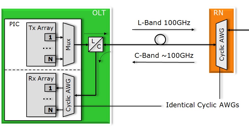
Photonic integration will also be used in emerging standards such as wavelength division multiplexing PON (WDM-PON), especially at the head-end where the optical line terminal (OLT) resides.
“WDM-PON is very much point-to-point even though the fibre is shared like a normal PON,” says David Smith, CTO at CIP Technologies. “When you get in the central office there is a mass of equipment just like point-to-point [access].” The opportunity is to integrate the OLT’s lasers – typically 32 or 64 - into arrays, which will also save power, says Smith.
Tunables and interconnects
Other market segments are benefiting from photonic integration besides 40 and 100Gbps transmission and PON.
JDS Uniphase’s XFP module-based tunable laser is possible by monolithically integration the laser and Mach-Zehnder modulator. Not only is the resulting tunable laser compact – it is a few millimeters long - such that it and the associated electronics fit within the module, but the power consumption is below the pluggable’s 3.5W ceiling.
JDS Uniphase has also developed a compact optical amplifier that extends long-haul optical transmission before electrical signal regeneration is needed. A PLC chip is used to replace some 50 discrete optical components including isolators, photo-detectors for signal monitoring, a variable pump splitter and tunable gain-flattening and tilt filters.
The result is an amplifier halved in size and simpler to make since the PLC removes the need to route and splice fibres linking the discretes. Moreover, JDS Uniphase can use different PLC manufacturing masks to enable specific functions for particular customers. This is the closest the optical world gets to a programmable IC.
 Towards 1 terabit-per-second interfaces: a hybrid integrated prototype as part of an NIST project involving CyOptics and Kotura. Click on the photo for more details
The emerging 40 and 100 Gigabit Ethernet interface standards are another area suited for future integration. “What is driving optical integration here is size,” says Eng. “How do you fit 100Gigabit in a 3x5 inch module? That is cutting the size in half and will require a lot of R&D effort.”
In particular, optical integration will be needed to implement the 40GBASE-LR4 Gigabit Ethernet standard within a QSFP module. “You can’t fit four TO can lasers and four TO can receivers into a QSFP module,” says Rochus.
It is the 40 and 100 Gigabit Ethernet market that is the higher end market that also interests Enablence. “The drivers for PON and 100 Gigabit may be different but it’s the same PLC technology,” says Pearson. A PON diplexer may integrate one laser and one detector, for 100G it’s ten lasers and ten detectors, he says.
What next?
“Bandwidth growth is forcing us to consider architectures not considered before,” says Alcatel Lucent’s Bucci. The system vendor is accelerating its integration activities, whether it is integrating two wavelength-selective switches in a package or developing ‘electro-optic engines’ that combine advanced modulation optics and digital signal processing.
Moreover, operators themselves are more open to networking change due to the tremendous challenges they face, says Bucci: “They are being freed to do more, to take more risks.”
Welch believes one significant development that PICs will enable – perhaps a couple of years out - is adding and dropping at the packet level, at every site in the core network. “This will enable lots of reconfigurability and much finer granularity, delivering another level of networking efficiency,” he says.
Is this leading to disruption - the equivalent of digital cameras on handsets? Time will tell.
Click here for a mindmap of this article in PDF form.
OneChip solution for Fibre-To-The-Home
 Jim Hjartarson, CEO of OneChip PhotonicsAn interview with Jim Hjartarson, CEO of OneChip Photonics
Q. In March 2009, OneChip raised $19.5m. How difficult is it nowadays for an optical component firm to receive venture capital funding?
A. Clearly, the venture capital community, given the current macroeconomic environment, is being selective about the new investments it makes in the technology market in general, and photonics in particular. However, if you can demonstrate that you have a unique approach to a problem that has not yet been solved, and that there is a large, untapped market opportunity, VCs will be interested in your value proposition.
Q. What is it about your company's business plan that secured the investment?
A. We believe OneChip Photonics has three fundamental advantages that resulted in our securing our initial two rounds of funding, which totaled $19.5 million:
- A truly breakthrough approach and technology that will remove the cost and performance barriers that have been impeding the ubiquitous deployment of Fiber-to-the-Home (FTTH) and enable new business and consumer broadband applications.
- A large, untapped market opportunity. Ovum estimates that the FTTx optical transceiver market will grow from $387 million by the end of 2009 to $594 million by the end of 2013. OneChip also is poised to introduce photonics integration into other high-volume business and consumer markets, where our breakthrough photonic integrated circuit (PIC) technology can reduce costs and improve performance. These markets could be orders of magnitude larger than the FTTx optical transceiver market.
- A seasoned and successful management team. OneChip has attracted top talent – from industry leading companies such as MetroPhotonics, Bookham, Catena Networks, Fiberxon, Nortel and Teknovus – who have successful track records of designing, manufacturing, marketing and selling transceivers, PICs and mass-market broadband access solutions.
Q. The passive optical networking (PON) transceiver market faces considerable pricing pressures. Companies use TO cans and manual labour or more sophisticated hybrid integration where the laser and photodetectors are dropped onto a common platform to meet various PON transceiver specifications. Why is OneChip pursuing indium phosphide-based monolithic integration and why will such an approach be cheaper than a hybrid platform that can address several PON standards?
A. Most current FTTH transceiver providers base their transceivers on either discrete optics or planar lightwave circuit (PLC) designs. These designs offer low levels of integration and require assembly from multiple parts. There is little technical differentiation among them. Rather, vendors must compete on the basis of who can assemble the parts in a slightly cheaper fashion. And there is little opportunity to further reduce such costs.
While more integrated than fully discrete optics-based designs, PLC designs still require discrete active components and the assembly of as many as 10 parts. Great care must be taken, during the manufacturing process, to align all parts of the transceiver correctly. And while packaging can be non-hermetic, these parts can fall out of alignment through thermal or mechanical stress. PLC designs also have proven to be an expensive alternative. For all of these reasons, the PON system vendors with which OneChip has engaged have indicated that they are not interested in deploying PLC-based designs.
OneChip Photonics is taking a new approach with its breakthrough PIC technology. OneChip is monolithically integrating all the functions required for an optical transceiver onto a single, indium phosphide (InP)-based chip. All active AND passive components of the chip – including the distributed-feedback (DFB) laser, optically pre-amplified detector (OPAD), wavelength splitter (WS), spot-size converter (SSC), and various elements of passive waveguide circuitry – are, uniquely, integrated in one epitaxial growth step, without re-growth or post-growth modification of the epitaxial material.
With respect to transmit performance, OneChip’s single-frequency DFB lasers will offer a superior performance – much more suitable for longer-reach and higher bit-rate applications – than competing Fabry-Perot (FP) lasers. With respect to receive performance, OneChip’s optically pre-amplified detectordesign is a higher gain-bandwidth solution than competing avalanche photodiode (APD) solutions. It also is a lower-cost solution, as it does not require a high-voltage power source.
OneChip’smonolithic photonic integrated circuits (PICs) have the smallest footprint on the market, the optical parts are aligned for life, and the parts are highly robust (resistant to vibration and other outside elements). Further, OneChip’s PICs are designed for automated mounting on a silicon optical bench, without requiring active alignment, using industry-standard, automated assembly processes – resulting in high yields of good devices.
Utilizing automated production processes, OneChip can maintain the highest production scalability (easily ramping up and down) in the industry and respond rapidly to customer needs. Standard production processes also mean reliable supplies to customers, at the lowest prices on the market.
Q. Several companies have explored integrated PON solutions and have either dismissed the idea or have come to market with impressive integrated designs only to ultimately fail (e.g. Xponent Photonics).Why are you confident OneChip will fare better?
As noted earlier, PLC designs developed by vendors such as Xponent are not fully integrated. PLC designs still require discrete active components and the assembly of as many as 10 parts, using a glass substrate. This results in poor yields and high costs.
OneChip is taking a fundamentally different approach. We are the only company in the optical access market that is monolithically integrating all the active and passive functions required for an optical transceiver onto a single, indium phosphide (InP)-based chip. This enables us to achieve low cost, high performance, high yields and high quality.
OneChip is one of only a few companies with new core intellectual property and advanced technology in the optical transceiver business that can sustain a competitive advantage over other optical component providers, which rely on conventional technology and assembly processes. Carriers and system providers recognize that an approach, which would eliminate assembly from multiple parts, is needed to lower the cost and improve the performance of transceivers, Optical Network Terminals (ONTs) and Optical Line Terminals (OLTs) in optical access networks. We believe OneChip’s fully integrated technology can help unleash the potential of FTTH and other mass-market optical communications applications.
Q. If integrated PON is a good idea why, in OneChip’s opinion, have silicon photonics startups so far ignored this market?
A. “Silicon photonics” designs face the inherent limitation that a laser cannot be implemented in silicon. Therefore, separate optical and electrical devices must be grown with different processes and then assembled together. With as many as 10 parts having to be interconnected on a ceramic substrate, the alignment, tuning and reliability issues can significantly add costs and reduce yields.
In addition, system providers and service providers need to be cognizant of the inherent performance limitations with transceivers built from discrete parts. While short-reach EPON transceivers already have been optimized down to below a U.S. $15 price, these implementations can only meet low-end performance requirements. Networks would require a switch to more costly transceivers to support longer-range EPON, 2.5G EPON, GPON or 10G PON. Because most service providers are looking to reap the payback benefits of their investments in fiber installations/retrofits over the shortest possible timeframes, it doesn’t make sense to risk adding the high cost of a forklift changeover of transceiver technology at some point during the payback period.
Q. PON with its high volumes has always been viewed as the first likely market for photonic integrated circuits (PICs). What will be the second?
A. OneChip recognizes that optical communications is becoming economically and technologically mandatory in areas outside of traditional telecommunications, such as optical interconnections in data centers and other short to ultra-short reach broadband optical networks. OneChip is poised to introduce photonics integration into these and other high-volume business and consumer markets, where our PIC technology can reduce costs and improve performance.
[End]
Click here tomore details on OneChip Photonics