
Optical transmission: sending more data over a greater reach
Keysight Technologies' chart plots the record-setting optical transmission systems of recent years.
The chart, compiled by Dr Fabio Pittalá, product planner, broadband and photonic center of excellence at Keysight, is an update of one previously published by Gazettabyte.
The latest chart adds data from last year’s conferences at OFC 2023 and ECOC 2023. And new optical transmission achievements can be expected at the upcoming OFC 2024 show, to be held in San Diego, CA in March.

Working at the limit of optical transmission performance

- Expect to see new optical transmission records at the upcoming ECOC 2023 conference.
- Keysight Technologies’ chart plots the record-setting optical transmission systems of recent years.
- The chart reveals optical transmission performance issues and the importance of the high-speed converters between the analogue and digital domains for test equipment and, by implication, for coherent digital signal processors (DSPs).
Engineers keep advancing optical systems to send more data across an optical fibre.
It requires advances in optical and electronic components that can process faster, higher-bandwidth signals, and that includes the most essential electronics part of all: the coherent DSP chip.
Coherent DSPs use state-of-the-art 5nm and 3nm CMOS chip manufacturing processes. The chips support symbol rates from 130-200 gigabaud (GBd). At 200GBd, the coherent DSP’s digital-to-analogue converters (DACs) and analogue-to-digital converters (ADCs) must operate at at least 200 giga samples-per-second (GSps) and likely closer to 250GSps. DACs drive the optical modulator in the optical transmission path while the ADCs are used at the optical receiver to recover the signal.
Spare a thought for the makers of test equipment used in labs that drive such coherent optical transmission systems. The designers must push their equipments’ DACs and ADCs to the limit to generate and sample the waveforms of these prototype next-generation optical transmission systems.
Optical transmission records
The recent history of record-setting optical transmission systems reveals the design challenges of coherent components and how ADC and DAC designs are evolving.
It is helpful to see how test equipment designers tackle ADC and DAC design, given the devices are a critical element of the coherent DSP, and when vendors are reluctant to detail how they achieve 200GBd baud rates using on-chip CMOS-based ADCs and DACs.
Nokia and Keysight Technologies published a post-deadline paper at the ECOC 2022 conference detailing the transmission of a 260GBd single-wavelength signal over 100km of fibre.
The system achieved the high baud rate using a thin-film lithium niobate modulator driven by Keysight’s M8199B arbitrary waveform generator. The M8199B uses a design consisting of two interleaved DACs to generate signals at 260GSps.
A second post-deadline ECOC 2022 paper, published by NTT, detailed the sending of over two terabits-per-second (Tbps) on a single wavelength. This, too, used Keysight’s M8199B arbitrary waveform generator.
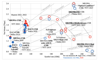
The chart above highlights optical transmission records since 2015, plotting the systems’ net bit rate – from 800 gigabits to 2.2 Tbps – against a symbol rate measured in GBd.
As with commercial coherent optical transport systems, the goal is to keep increasing the symbol rate. A higher symbol rate sends more data over the same fibre spans. For example, the 400ZR coherent transmission standard uses a symbol rate of some 60GBd to send a 400Gbps wavelength, while 800ZR doubles the baud rate to some 120GBd to transmit 800Gbps over similar distances.
“With the 1600ZR project just started by the OIF, this trend will likely continue,” says Fabio Pittalá, product planner, broadband and photonic center of excellence at Keysight.
The signal generator test equipment options include the use of different materials – CMOS and silicon germanium – and moving from one DAC to a parallel multiplexed DAC design.
Single DACs
In 2017, Nokia achieved a 1Tbps transmission using a 100GBd symbol rate. Nokia used a Micram 6-bit 100GSps DAC in silicon germanium for the modulation.
For its next advancement in transmission performance, in 2019, Nokia used the same DAC but a faster ADC at the receiver, moving from a Tektronix instrument using a 70GHz ADC to the Keysight UXR oscilloscope with a 110GHz bandwidth ADC. The resulting net bit rate was nearly 1.4 terabits.
Keysight also developed the M8194A arbitrary waveform generator based on a CMOS-based DAC. The higher sampling rate of this arbitrary waveform generator increased the baud rate to 105GBd, but because of the bandwidth limitation, the net bit rate was lower.
The bandwidth of CMOS DACs can be improved but it tops out in the region of 50-60GHz. “It’s very difficult to scale to a higher baud rate using this technology,” says Pittalá. Silicon germanium, by contrast, supports much higher bandwidths but has a higher power consumption.
In 2020, Nokia reached 1.6Tbps at 128GBd using the Micram DAC5, an 8-bit 128GSps DAC based on silicon germanium. A year later, Keysight released the M8199A arbitrary waveform generator. “This was also based on 8-bit silicon germanium DACs operating at 128GSps, but the signal-to-noise ratio was greatly improved, allowing to generate higher-order quadrature amplitude modulation formats with more than sixteen levels,” says Pittalá.
This arbitrary waveform generator was used in systems that, coupled with advanced equalisation schemes, pushed the net bit rate to almost 2Tbps.
Going parallel
For the subsequent advances in baud rate, parallel DAC designs, multiplexing two or more DACs together, were implemented by different research labs.
In 2015, NTT multiplexed two DACs that advanced the symbol rate from 105GBd to 120GBd. In 2019, NTT moved to a different type of multiplexer, which, used with the same DAC, increased the baud rate to around 170GBd. Nokia also demonstrated a multiplexed design concept, which, together with a novel thin-film lithium niobate modulator, extended the symbol rate to 200GBd, achieving a 1.6Tbps net bit rate.
Last year, Keysight introduced its latest arbitrary waveform generator, the M8199B. The design also adopted a multiplexed DAC design.
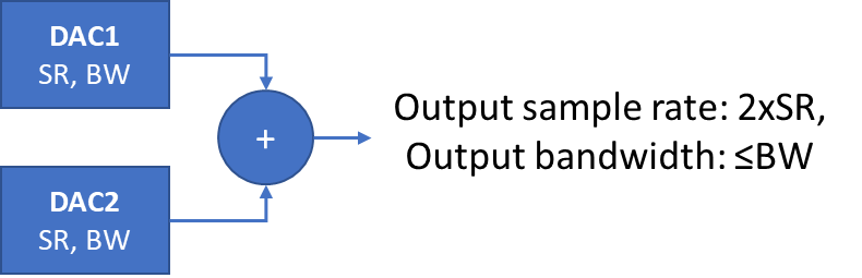
Multiplexing two DACs. SR refers to sample rate, BW refers to bandwidth. Source: Keysight.
“There are two 128GSps 8-bit silicon germanium DACs that are time-interleaved to get a higher speed signal per dimension,” says Pittalá. If the two DACs are shifted in time and added together, the result is a higher sampling rate overall. However, Pittalá points out that while the sample rate is effectively doubled, the overall bandwidth is defined by the individual DACs (see diagram above).
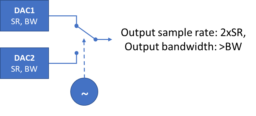
Pittalá also mentions another technique, based on active clocking, that does increase the bandwidth of the system. The multiplexer is clocked and acts like a fast switch between the two DAC channels. “In principle, you can double the bandwidth, ” he says. (See diagram below.)
The Keysight’s M8199B’s improved performance, combined with advances in components such as NTT’s 130GHz indium phosphide amplifier, resulted in over 2Tbps transmission, as detailed in the ECOC 2022 paper. As the baud rate was increased, the modulation scheme used and the net bit rate decreased. (Shown by the red dots on the chart).
In parallel, Keysight worked with Nokia, which used a thin-film lithium niobate modulator for their set-up, a different modulator to NTT’s. The test equipment directly drove the thin-film modulator; no external modulator driver was needed. The system was operated as high as 260GBd, achieving a net bit rate of 800Gbps.
Pittalà notes that while the NTT system differs from Nokia’s, Nokia’s two red points on the extreme right of the chart continue the trajectory of NTT’s six red points as the baud rate increases.
OFC’23 O-band record
The post-deadline papers at the OFC 2023 conference earlier this year did not improve the transmission performances of the ECOC papers.
A post-deadline paper published at OFC 2023 showed a record of coherent transmission in the O-Band. Working with Keysight, McGill University showed 1.6Tbps coherent transmission over 10km using a thin-film lithium niobate modulator. The system operated at 167GBd, used a 64-QAM modulation scheme, and used the Keysight M8199B.
Pittalà expects that at ECOC 2023, to be held in Glasgow in October, new record-breaking transmissions will be announced.
His chart will need updating.
Further information
Thin-film lithium niobate modulators, click here

FSAN close to choosing the next generation of PON
Briefing: Next-gen PON
Part 1: NG-PON2
The next-generation passive optical network (PON) will mark a departure from existing PON technologies. Some operators want systems based on the emerging standard for deployment by 2015.

“One of the goals in FSAN is to converge on one solution that can serve all the markets"
Derek Nesset, co-chair of FSAN's NGPON task group
The Full Service Access Network (FSAN) industry group is close to finalising the next optical access technology that will follow on from 10 Gigabit GPON.
FSAN - the pre-standards forum consisting of telecommunications service providers, testing labs and equipment manufacturers - crafted what became the International Telecommunication Union's (ITU) standards for GPON (Gigabit PON) and 10 Gigabit GPON (XGPON1). In the past year FSAN has been working on NG-PON2, the PON technology that comes next.
“One of the goals in FSAN is to converge on one solution that can serve all the markets - residential users, enterprise and mobile backhaul," says Derek Nesset, co-chair of FSAN's NGPON task group.
Some mobile operators are talking about backhaul demands that will require multiple 10 Gigabit-per-second (Gbps) links to carry the common public radio interface (CPRI), for example. The key design goal, however, is that NG-PON2 retains the capability to serve residential users cost-effectively, stresses Nesset.
FSAN says it has a good description of each of the candidate technologies: what each system looks like and its associated power consumption. "We are trying to narrow down the solutions and the ideal is to get down to one,” says Nesset.
The power consumption of the proposed access scheme is of key interest for many operators, he says. Another consideration is the risk associated with moving to a novel architecture rather than adopting an approach that builds on existing PON schemes.
Operators such as NTT of Japan and Verizon in the USA have a huge installed base of PON and want to avoid having to amend their infrastructure for any next-generation PON scheme unable to re-use power splitters. Other operators such as former European incumbents are in the early phases of their rollout of PON and have Greenfield sites that could deploy other passive infrastructure technologies such as arrayed waveguide gratings (AWG).
"The ideal is we select a system that operates with both types of infrastructure," says Nesset. "Certain flavours of WDM-PON (wavelength division multiplexing PON) don't need the wavelength splitting device at the splitter node; some form of wavelength-tuning can be installed at the customer premises." That said, the power loss of existing optical splitters is higher than AWGs which impacts PON reach – one of several trade-offs that need to be considered.
Once FSAN has concluded its studies, member companies will generate 'contributions' for the ITU, intended for standardisation. The ITU has started work on defining high-level requirements for NG-PON2 through contributions from FSAN operators. Once the NG-PON2 technology is chosen, more contributions that describe the physical layer, the media access controller and the customer premise equipment's management requirements will follow.
Nesset says the target is to get such documents into the ITU by September 2012 but achieving wide consensus is the priority rather than meeting this deadline. "Once we select something in FSAN, we expect to see the industry ramp up its contributions based on that selected technology to the ITU," says Nesset. FSAN will select the NG-PON2 technology before September.
NG-PON2 technologies
Candidate technologies include an extension to the existing GPON and XGPON1 based on time-division multiplexing (TDM). Already vendors such as Huawei have demonstrated prototype 40 Gigabit capacity PON systems that also support hybrid TDM and WDM-PON (TWDM-PON). Other schemes include WDM-PON, ultra-dense WDM-PON and orthogonal frequency division multiplexing (OFDM).
Nesset says there are several OFDM variants being proposed. He views OFDM as 'DSL in the optical domain’: sub-carriers finely spaced in the frequency domain, each carrying low-bit-rate signals.
One advantage of OFDM technology, says Nesset, includes taking a narrowband component to achieve a broadband signal: a narrowband 10Gbps transmitter and receiver can achieve 40Gbps using sub-carriers, each carrying quadrature amplitude modulation (QAM). "All the clever work is done in CMOS - the digital signal processing and the analogue-to-digital conversion," he says. The DSP executes the fast Fourier transform (FFT) and the inverse FFT.
"We are trying to narrow down the solutions and the ideal is to get down to one"
Another technology candidate is WDM-PON including an ultra-dense variant that promises a reach of up to 100km and 1,000 wavelengths. Such a technology uses a coherent receiver to tune to the finely spaced wavelengths.
In addition to being compatible with existing infrastructure, another FSAN consideration is compatibility with existing PON standards. This is to avoid having to do a wholesale upgrade of users. For example, with XGPON1, the optical line terminal (OLT) using an additional pair of wavelengths - a wavelength overlay - sits alongside the existing GPON OLT. ”The same principle is desirable for NG-PON2,” says Nesset.
However, an issue is that spectrum is being gobbled up with each generation of PON. PON systems have been designed to be low cost and the transmit lasers used are not wavelength-locked and drift with ambient temperature. As such they consume spectrum similar to coarse WDM wavelength bands. Some operators such as Verizon and NTT also have a large installed base of analogue video overlay at 1550nm.
”So in the 1500 band you've got 1490nm for GPON, 1550nm for RF (radio frequency) video, and 1577nm for XGPON; there are only a few small gaps,” says Nesset. A technology that can exploit such gaps is both desirable and a challenge. “This is where ultra-dense WDM-PON could come into play,” he says. This technology could fit tens of channels in the small remaining spectrum gaps.
The technological challenges implementing advanced WDM-PON systems that will likely require photonic integration is also a concern for the operators. "The message from the vendors is that ’when you tell us what to do, we have got the technology to do it’,” says Nesset. ”But they need the see the volume applications to justify the investment.” However, operators need to weigh up the technological risks in developing these new technologies and the potential for not realising the expected cost reductions.
Timetable
Nesset points out that each generation of PON has built on previous generations: GPON built on BPON and XGPON on GPON. But NG-PON2 will inevitably be based on new approaches. These include TWDM-PON which is an evolution of XG-PON into the wavelength domain, virtual point-to-point approaches such as WDM-PON that may also use an AWG, and the use of digital signal processing with OFDM or coherent ultra dense WDM-PON. ”It is quite a challenge to weigh up such diverse technological approaches,” says Nesset.
If all goes smoothly it will take two ITU plenary meetings, held every nine months, to finalise the bulk of the NG-PON2 standard. That could mean mid-2013 at the earliest.
FSAN's timetable is based on operators wanting systems deployable in 2015. That requires systems to be ready for testing in 2014.
“[Once deployed] we want NG-PON2 to last quite a while and be scalable and flexible enough to meet future applications and markets as they emerge,” says Nesset.