
How scaling optical networks is soon to change
Carrier division multiplexing and spatial division multiplexing (CSDM) are both needed, argues Lumentum’s Brian Smith.
The era of coherent-based optical transmission as is implemented today is coming to an end, argues Lumentum in a White Paper.

Brian Smith
The author of the paper, Brian Smith, product and technology strategy, CTO Office at Lumentum, says two factors account for the looming change.
One is Shannon’s limit that defines how much information can be sent across a communications channel, in this case an optical fibre.
The second, less discussed regarding coherent-based optical transport, is how Moore’s law is slowing down.
”Both are happening coincidentally,” says Smith. “We believe what that means is that we, as an industry, are going to have to change how we scale capacity.”
Accommodating traffic growth
A common view in telecoms, based on years of reporting, is that internet traffic is growing 30 per cent annually. The CEO of AT&T mentioned over 30 per cent traffic growth in its network for the last three years during the company’s last quarterly report of 2023.
Smith says that data on the rate of traffic growth is limited. He points to a 2023 study by market research firm TeleGeography that shows traffic growth is dependent on region, ranging from 25 to 45 per cent CAGR.
Since the deployment of the first optical networking systems using coherent transmission in 2010, almost all networking capacity growth has been achieved in the C-band of a fibre, which comprises approximately 5 terahertz (THz) of spectrum.
Cramming more data into the C-band has come about by increasing the symbol rate used to transmit data and the modulation scheme used by the coherent transceivers, says Smith.
 The current coherent era – labelled the 5th on the chart – is coming to an end. Source: Lumentum.
Pushing up baud rate
Because of the Shannon limit being approached, marginal gains exist to squeeze more data within the C-band. It means that more spectrum is required. In turn, the channel bandwidth occupied by an optical wavelength now goes up with baud rate such that while each wavelength carries more data, the capacity limit within the C-band has largely been reached.
Current systems use a symbol rate of 130-150 gigabaud (GBd). Later this year Ciena will introduce its 200GBd WaveLogic 6e coherent modem, while the industry has started work on developing the next generation 240-280GBd systems.
Reconfigurable optical add-drop multiplexers (ROADMs) have had to become ‘flexible’ in the last decade to accommodate changing channel widths. For example, a 400-gigabit wavelength fits in a 75GHz channel while an 800-gigabit wavelength fits within a 150GHz channel.
Another consequence of Shannon’s limit is that the transmission distance limit for a certain modulation scheme has been reached. Using 16-ary quadrature amplitude modulation (16-QAM), the distance ranges from 800-1200km. Doubling the baud rate doubles the data rate per wavelength but the link span remains fixed.
“There is a fundamentally limit to the maximum reach that you can achieve with that modulation scheme because of the Shannon limit,” says Smith.
At the recent OFC show held in March in San Diego, a workshop discussed whether a capacity crunch was looming.
The session’s consensus was that, despite the challenges associated with the latest OIF 1600ZR and ZR+ standards, which promise to send 1.6 terabits of data on a single wavelength, the industry is confident that it will meet the OIF’s 240-280+ GBd symbol rates.
However, in the discussion about the next generation of baud rate—400-500GBd—the view is that while such rates look feasible, it is unclear how they will be achieved. The aim is always to double baud rate because the increase must be meaningful.
“If the industry can continue to push the baud rate, and get the cost-per-bit, power-per-bit, and performance required, that would be ideal,” says Smith.
But this is where the challenges of Moore’s law slowing down comes in. Achieving 240GBd and more will require a coherent digital signal processor (DSP) made using a 3nm CMOS process at least. Beyond this, transistors start to approach atomic scale and the performance becomes less deterministic. Moreover, the development costs of advanced CMOS processes – 3nm, 2nm and beyond – are growing exponentially.
Beyond 240GBd, it’s also going to become more challenging to achieve the higher analogue bandwidths for the electronics and optics components needed in a coherent modem, says Smith. How the components will be packaged is key. There is no point in optimising the analogue bandwidth of each component only for the modem performance to degrade due to packaging. “These are massive challenges,” says Smith.
This explains why the industry is starting to think about alternatives to increasing baud rate, such as moving to parallel carriers. Here a coherent modem would achieve a higher data rate by implementing multiple wavelengths per channel.
Lumentum refers to this approach as carrier division multiplexing.
Capacity scaling
The coherent modem, while key to optical transport systems, is only part of the scaling capacity story.
Prior to coherent optics, capacity growth was achieved by adding more and more wavelengths in the C-band. But with the advent of coherent DSPs compensating for chromatic and polarisation mode dispersion, suddenly baud rate could be increased.
“We’re starting to see the need, again, for growing spectrum,” says Smith. “But now, we’re growing spectrum outside the C-band.”
First signs of this are how optical transport systems are adding the L-band alongside the C-band, doubling a fibre’s spectrum from five to 10THz.
“The question we ask ourselves is: what happens once the C and L bands are exhausted?” says Smith.
Lumentum’s belief is that spatial division multiplexing will be needed to scale capacity further, starting with multiple fibre pairs. The challenge will be how to build systems so that costs don’t scale linearly with each added fibre pair.
There are already twin wavelength selective switches used for ROADMs for the C-band and L-bands. Lumentum is taking a first step in functional integration by combining the C- and L-bands in a single wavelength selective switch module, says Smith. “And we need to keep doing functional integration when we move to this new generation where spatial division multiplexing is going to be the approach.”
Another consideration is that, with higher baud-rate wavelengths, there will be far fewer channels per fibre. And with growing fibre pairs per route, that suggests a future need for fibre-switched networking not just wavelength switching networking as used today.
“Looking into the future, you may find that your individual routeable capacity is closer to a full C-band,” says Smith.
Will carrier division multiplexing happen before spatial division multiplexing?
Smith says that spatial division multiplexing will likely be first because Shannon’s limit is fundamental, and the industry is motivated to keep pushing Moore’s law and baud rate.
“With Shannon’s limit and with the expansion from C-band to C+L Band, if you’re growing at that nominal 30 per cent a year, a single fibre’s capacity will exhaust in two to three years’ time,” says Smith. “This is likely the first exhaust point.”
Meanwhile, even with carrier division multiplexing and the first parallel coherent modems after 240GBd, advancing baud rate will not stop. The jumps may diminish from the doublings the industry knows and that will continue for several years yet. But they will still be worth having.

IoT will drive chip design and new styles of computing
Looking back 20 years hence, how will this period be viewed? The question was posed by the CEO of imec, Luc Van de hove, during his opening talk at a day event imec organised in Tel-Aviv.
For Van den hove, this period will be seen as one of turbulent technological change. “The world is changing at an incredible rate,” he says. “The era of digital disruption is changing our industry and this disruption is not going to stop.”
 Luc Van den hove
It was the Belgium nonoelectronics R&D centre’s second visit to Israel to promote its chip and systems expertise as it seeks to expand its links with Israel’s high-tech industry. And what most excites imec is the Internet of Things (IoT), the advent of connected smart devices that turn data into information and adapt the environment to our needs.
The world is changing at an incredible rate. The era of digital disruption is changing our industry and this disruption is not going to stop
Internet of Things
Imec is focussing on five IoT areas: Smart Health - wearable and diagnostic devices, Smart Mobility which includes technologies for autonomous cars, drones and robots, Smart Cities, Smart Industry and Smart Energy. “In all these areas we look at how we can leverage our semiconductor know-how,” says Van den hove. “How we can bring innovative solutions by using our microchip technology.”
The broad nature of the IoT means imec must form partnerships across industries while strengthening its systems expertise. In healthcare, for example, imec is working with John Hopkins University, while last October, imec completed the acquisition of iMinds, a Belgium research centre specialising in systems software and security.
“One of the challenges of IoT is that there is not one big killer application,” says Van den hove. “How to bring these technologies to market is a challenge.” And this is where start-ups can play a role and explains why imec is visiting Israel, to build its partnerships with local high-tech firms.
Imec also wants to bring its own technologies to market through start-ups and has established a €100 million investment fund to incubate new ideas and spin-offs.
Technologies
Imec’s expertise ranges from fundamental semiconductor research to complex systems-on-chip. It is focussing on advanced sensor designs for IoT as this is where it feels it can bring an advantage. Imec detailed a radar chip design for cars that operates at 79GHz yet is implemented in CMOS. It is also developing a Light Detection and Ranging (LIDAR) chip for cars based on integrated photonics. Future cars will have between 50 to 100 sensors including cameras, LIDAR, radar and ultrasound.
 Imec's multi-project wafers. Source: imec
The data generated from these sensors must be processed, fused and acted upon. Imec is doing work in the areas of artificial intelligence and machine learning. In particular, it is developing neuromorphic computing devices that use analogue circuits to mimic the biological circuitry of the brain. Quantum computing is another area imec has begun to explore.
One of the challenges of IoT is that there is not one big killer application
“There is going to be so much data generated,” says Van den Hove. “And it is better to do it [processing] locally because computation is cheaper than bandwidth.”
Imec envisages a network with layers of intelligence, from the sensors all the way to the cloud core. As much of the data as possible will be processed by the sensor so that it can pass on more intelligent information to the network edge, also known as fog computing. Meanwhile, the cloud will be used for long-term data storage, for historical trending and for prediction using neuromorphic algorithms, says Van den Hove.
But to perform intensive processing on-chip and send the results off-chip in a power-efficient manner will require advances in semiconductor technology and the continuation of Moore’s law.
Moore's law
Imec remains confident that Moore’s law will continue to advance for some years yet but notes it is getting harder. In the past, semiconductor technology had a predictable roadmap such that chip designers could plan ahead and know their design goals would be met. Now chip technologists and designers must work together, a process dubbed technology-design co-optimisation.
Van den hove cites the example of imec’s work with ARM Holdings to develop a 7nm CMOS process node. “You can create some circuit density improvement just by optimising the design, but you need some specific technology features to do that,” he says. For example, by using a self-alignment technique, fewer metal tracks can be used when designing a chip's standard cell circuitry. "Using the same pitch you get an enormous shrink," he says. But even that is not going to be enough and techniques such as system-technology co-optimisation will be needed.
Imec is working on FinFETs, a style of transistor, to extend CMOS processes down to 5nm and then sees the use of silicon nanowire technology - first horizontal and then vertical designs - to extend the roadmap to 3nm, 2.5nm and even 1.8nm feature sizes.
Imec is also working on 3D chip stacking techniques that will enable multi-layer circuits to be built. “You can use specific technologies for the SRAM, processing cores and the input-output.” Imec is an active silicon photonics player, seeing the technology playing an important role for optical interconnect.
Imec awarded Gordon Moore a lifetime of innovation award last year, and Van den hove spent an afternoon at Moore’s home in Hawaii. Van den hove was struck with Moore’s humility and sharpness: “He was still so interested in the technology and how things were going.”
Tackling system design on a data centre scale
Interview 1: Andrew Rickman
Silicon photonics has been a recurring theme in the career of Andrew Rickman. First, as a researcher looking at the feasibility of silicon-based optical waveguides, then as founder of Bookham Technologies, and after that as a board member of silicon photonics start-up, Kotura.
 Andrew Rickman
Now as CEO of start-up Rockley Photonics, his company is using silicon photonics alongside its custom ASIC and software to tackle a core problem in the data centre: how to connect more and more servers in a cost effective and scaleable way.
Origins
As a child, Rickman attended the Royal Institution Christmas Lectures given by Eric Laithwaite, a popular scientist who was also a professor of electrical engineering at Imperial College. As an undergraduate at Imperial, Rickman was reacquainted with Professor Laithwaite who kindled his interest in gyroscopes.
“I stumbled across a device called a fibre-optic gyroscope,” says Rickman. “Within that I could see people starting to use lithium niobate photonic circuits.” It was investigating the gyroscope design and how clever it was that made Rickman wonder whether the optical circuits of such a device could be made using silicon rather than exotic materials like lithium niobate.
“That is where the idea triggered, to look at the possibility of being able to make optical circuits in silicon,” he says.
If you try and force a photon into a space shorter than its wavelength, it behaves very badly
In the 1980s, few people had thought about silicon in such a context. That may seem strange today, he says, but silicon was not a promising candidate material. “It is not a direct band-gap material - it was not offering up the light source, and it did not have a big electro-optic effect like lithium niobate which was good for modulators,” he says. “And no one had demonstrated a low-loss single-mode waveguide.”
Rickman worked as a researcher at the University of Surrey’s physics department with such colleagues as Graham Reed to investigate whether the trillions of dollars invested in the manufacturing of silicon could also be used to benefit photonic circuits and in particular whether silicon could be used to make waveguides. “The fundamental thing one needed was a viable waveguide,” he says.
Rickman even wrote a paper with Richard Soref who was collaborating with the University of Surrey at the time. “Everyone would agree that Richard Soref is the founding father of the idea - the proposal of having a useful waveguide in silicon - which is the starting point,” says Rickman. It was the work at the University of Surrey, sponsored by Bookham which Rickman had by then founded, that demonstrated low-loss waveguides in silicon.
Fabrication challenges
Rickman argues that not having a background in CMOS processes has been a benefit. “I wasn’t dyed-in-the-wool-committed to CMOS-type electronics processing,” he says. “I looked upon silicon technology as a set of machine-shop processes for making things.”
Looking at CMOS processing completely afresh and designing circuits optimised for photonics yielded Bookham a great number of high-performance products, he says. In contrast, the industry’s thrust has been very much a semiconductor CMOS-focused one. “People became interested in photonics because they just naturally thought it was going to be important in silicon, to perpetuate Moore’s law,” says Rickman.
You can use the structures and much of the CMOS processes to make optical waveguides, he says, but the problem is you create small structures - sub-micron - that guide light poorly. “If you try and force a photon into a space shorter than its wavelength, it behaves very badly,” he says. “In microelectronics, an electron has got a wavelength that is one hundred times smaller that the features it is using.”
The results include light being sensitive to interface roughness and to the manufacturing tolerances - the width, hight and composition of the waveguide. “At least an order of magnitude more difficult to control that the best processes that exist,” says Rickman.
“Our [Rockley’s] waveguides are one thousand times more relaxed to produce than the competitors’ smaller ones,” he says. “From a process point of view, we don’t need the latest CMOS node, we are more a MEMS process.”
If you take control of enough of the system problem, and you are not dictated to in terms of what MSA or what standard that component must fit into, and you are not competing in this brutal transceiver market, then that is when you can optimise the utilisation of silicon photonics
Rickman stresses that small waveguides do have merits - they go round tighter bends, and their smaller-dimensioned junctions make for higher-speed components. But using very large features solves the ‘fibre connectivity problem’, and Rockley has come up with its own solutions to achieve higher-speed devices and dense designs.
“Bookham was very strong in passive optics and micro-engineered features,” says Rickman. “We have taken that experience and designed a process that has all the advantages of a smaller process - speed and compactness - as well as all the benefits of a larger technology: the multiplexing and demultiplexing for doing dense WDM, and we can make a chip that already has a connector on it.”
Playing to silicon photonics’ strengths
Rickman believes that silicon photonics is a significant technological development: “It is a paradigm shift; it is not a linear improvement”. But what is key is how silicon photonics is applied and the problem it is addressing.
To make an optical component for an interface standard or a transceiver MSA using silicon photonics, or to use it as an add-on to semiconductors - a ’band-aid” – to prolong Moore’s law, is to undersell its full potential. Instead, he recommends using silicon photonics as one element - albeit an important one - in an array of technologies to tackle system-scale issues.
“If you take control of enough of the system problem, and you are not dictated to in terms of what MSA or what standard that component must fit into, and you are not competing in this brutal transceiver market, then that is when you can optimise the utilisation of silicon photonics,” says Rickman. “And that is what we are doing.” In other words, taking control of the environment that the silicon sits in.
It [silicon photonics] is a paradigm shift; it is not a linear improvement
Rockley’s team has been structured with the view to tackle the system-scale problem of interconnecting servers in the data centre. Its team comprises computer scientists, CMOS designers - digital and analogue - and silicon photonics experts.
Knowing what can be done with the technologies and organising them allows the problems caused by the ‘exhaustion of Moore’s law’ and the input/output (I/O) issues that result to be overcome. “Not how you apply one technology to make up for the problems in another technology,” says Rickman.
The ending of Moore’s law
Moore’s law continues to deliver a doubling of transistors every two years but the associated scaling benefits like the halving of power consumed per transistor no longer apply. As a result, while Moore’s law continues to grow gate count that drives greater computation, the overall power consumption is no longer constant.
Rickman also points out that the I/O - the number of connections on and off a chip - are not doubling with transistor count. “I/O may be going from 25 gigabit to 50 gigabit using PAM–4 but there are many challenges and the technology has yet to be demonstrated,” he says.
The challenge facing the industry is that increasing the I/O rate inevitably increases power consumption. “As power consumption goes up, it also equates to cost,” says Rickman. Clearly that is unwelcome and adds cost, he says, but that is not the only issue. As power goes up, you cannot fully benefit from the doubling transistor counts, so things cannot be packed more densely.
“You are running into to the end of Moore’s law and you don’t get the benefit of reducing space and cost because you’ve got to bolt on all these other things as it is very difficult to get all these signals off-chip,” he says.
This is where tackling the system as a whole comes in. You can look at microelectronics in isolation and use silicon photonics for chip-to-chip communications across a printed circuit board to reduce the electrical losses through the copper traces. “A good thing to do,” stresses Rickman. Or you can address, as Rockley aims to do, Moore’s law and the I/O limitations within a complete system the size of the data centre that links hundred of thousands of computers. “Not the same way you’d solve an individual problem in an individual device,” says Rickman.
Rockley Photonics
Rockley Photonics has already demonstrated all the basic elements of its design. “That has gone very well,” says Rickman.
The start-up has stated its switch design uses silicon photonics for optical switching and that the company is developing an accompanying controller ASIC. It has also developed a switching protocol to run on the hardware. Rockley’s silicon photonics design performs multiplexing and demultiplexing, suggesting that dense WDM is being used as well as optical switching.
Rockley is a fabless semiconductor company and will not be building systems. Partly, it is because it is addressing the data centre and the market has evolved in a different way to telecoms. For the data centre, there are established switch vendors and white-box manufacturers. As such, Rockley will provide its chipset-based reference design, its architecture IP and the software stack for its customers. “Then, working with the customer contract manufacturer, we will implement the line cards and the fabric cards in the format that the particular customer wants,” says Rickman.
The resulting system is designed as a drop-in replacement for the large-scale data centre players’ switches they haver already deployed, yet will be cheaper, more compact and consume less power, says Rockley.
“They [the data centre operators] can scale the way they do at the moment, or they can scale with our topology,” says Rickman.
The start-up expects to finally unveil its technology by the year end.
Imec gears up for the Internet of Things economy
It is the imec's CEO's first trip to Israel and around us the room is being prepared for an afternoon of presentations the Belgium nanoelectronics research centre will give on its work in such areas as the Internet of Things and 5G wireless to an audience of Israeli start-ups and entrepreneurs.
 Luc Van den hove
iMinds merger
Imec announced in February its plan to merge with iMinds, a Belgium research centre specialising in systems software and security, a move that will add 1,000 staff to imec's 2,500 researchers.
At first glance, the world-renown semiconductor process technology R&D centre joining forces with a systems house is a surprising move. But for Van den hove, it is a natural development as the company continues to grow from its technology origins to include systems-based research.
"Over the last 15 years we have built up more activities at the system level," he says. "These include everything related to the Internet of Things - our wireless and sensor programmes; we have a very strong programme on biomedical applications, which we sometimes refer to as the Internet of Healthy Things - wearable and diagnostics devices, but always leveraging our core competency in process technology."
Imec is also active in energy research: solar cells, power devices and now battery technology.
For many of these systems R&D programmes, an increasing challenge is managing data. "If we think about wearable devices, they collect data all the time, so we need to build up expertise in data fusion and data science topics," says Van den hove. There is also the issue of data security, especially regarding personal medical data. Many security solutions are embedded in software, says Van den hove, but hardware also plays a role.
Imec expects the Internet of Things to generate massive amounts of data, and more and more intelligence will need to be embedded at different levels in the network
"It just so happens that next to imec we have iMinds, a research centre that has top expertise in these areas [data and security]," says Van den hove. "Rather than compete with them, we felt it made more sense to just merge."
The merger also reflects the emergence of the Internet of Things economy, he says, where not only will there be software development but also hardware innovation: "You need much more hardware-software co-development". The merger is expected to be completed in the summer.
Internet of Things
Imec expects the Internet of Things to generate massive amounts of data, and more and more intelligence will need to be embedded at different levels in the network.
"Some people refer to it as the fog - you have the cloud and then the fog, which brings more data processing into the lower parts of the network," says Van den hove. "We refer to it as the Intuitive Internet of Things with intelligence being built into the sensor nodes, and these nodes will understand what the user needs; it is more than just measuring and sending everything to the cloud."
Van den hove says some in the industry believe that these sensors will be made in cheap, older-generation chip technologies and that processing will be performed in data centres. "We don't think so," he says. "And as we build in more intelligence, the sensors will need more sophisticated semiconductors."
Imec's belief is that the Internet of Things will be a driver for the full spectrum of semiconductor technologies. "This includes the high-end [process] nodes, not only for servers but for sophisticated sensors," he says.
"In the previous waves of innovation, you had the big companies dominating everything," he says. "With the Internet of Things, we are going to address so many different markets - all the industrial sectors will get innovation from the Internet of Things." There will be opportunities for the big players but there will also be many niche markets addressed by start-ups and small to medium enterprises.
Imec's trip to Israel is in response to the country's many start-ups and its entrepreneurship. "Especially now with our wish to be more active in the Internet of Things, we are going to work more with start-ups and support them," he says. "I believe Israel is an extremely interesting area for us in the broad scope of the Internet of Things: in wireless and all these new applications."
 Herzliya
Semiconductor roadmap
Van den hove's background is in semiconductor process technology. He highlights the consolidation going on in the chip industry due, in part, to the CMOS feature nodes becoming more complex and requiring greater R&D expenditure to develop, but this is a story he has heard throughout his career.
"It always becomes more difficult - that is Moore's law - and [chip] volumes compensate for those challenges," says Van den hove. When he started his career 30 years ago the outlook was that Moore's law would end in 10 years' time. "If I talk to my core CMOS experts, the outlook is still 10 years," he says.
Imec is working on 7nm, 5nm and 3nm feature-size CMOS process technologies. "We see a clear roadmap to get there," he says. He expects the third dimension and stacking will be used more extensively, but he does not foresee the need for new materials like graphene or carbon nanotubes being used for the 3nm process node.
Imec is pursuing finFET transistor technology and this could be turned 90 degrees to become a vertical nanowire, he says. "But this is going to be based on silicon and maybe some compound semiconductors like germanium and III-V materials added on top of silicon." The imec CEO believes carbon-based materials will appear only after 3nm.
"The one thing that has to happen is that we have a cost-effective lithography technique and so EUV [extreme ultraviolet lithography] needs to make progress," he says. Here too he is upbeat pointing to the significant progress made in this area in the last year. "I think we are now very close to real introduction and manufacturing," he says.
We see strong [silicon photonics] opportunities for optical interconnect and that is one of our biggest activities, but also sensor technology, particularly in the medical domain
Silicon Photonics
Silicon photonics is another active research area with some 200 staff at imec and at its associated laboratory at Ghent university. "We see strong opportunities for optical interconnect and that is one of our biggest activities, but also sensor technology, particularly in the medical domain," he says.
Imec views silicon photonics as an evolutionary technology. "Photonics is being used at a certain level of a system now and, step by step, it will get closer to the chip," he says. "We are focussing more on when it will be on the board and on the chip."
Van den hove talks about integrating the photonics on a silicon interposer platform to create a cost-effective solution for the printed circuit board and chip levels. For him, first applications of such technology will be at the highest-end technologies of the data centre.
For biomedical sensors, silicon photonics is a very good detector technology. "You can grow molecules on top of the photonic components and by shining light through them you can perform spectroscopy; the solution is extremely sensitive and we are using it for many biomedical applications," he says.
Looking forward, what most excites Van den hove is the opportunity semiconductor technology has to bring innovation to so many industrial sectors: "Semiconductors have created a fantastic revolution is the way we communicate and compute but now we have an opportunity to bring innovation to nearly all segments of industry".
He cites medical applications as one example. "We all know people that have suffered from cancer in our family, if we can make a device that would detect cancer at a very early stage, it would have an enormous impact on our lives."
Van den hove says that while semiconductors is a mature technology, what is happening now is that semiconductors will miniaturise some of the diagnostics devices just like has happened with the cellular phone.
"We are developing a single chip that will allow us to do a full blood analysis in 10 minutes," he says. DNA sequencing will also become a routine procedure when visiting a doctor. "That is all going to be enabled by semiconductor technology."
Such developments is also a reflection of how various technologies are coming together: the combination of photonics with semiconductors, and the computing now available.
Imec is developing a disposable chip designed to find tumour cells in the blood that requires the analysis of thousands of images per second. "The chip is disposable but the calculations will be done on a computer, but it is only with the most advanced technology that you can do that," says Van den hove.
Interconnection networks - an introduction
 Source: Jonah D. Friedman
If moving information between locations is the basis of communications, then interconnection networks represent an important subcategory.
The classic textbook, Principles and Practices of Interconnection Networks by Dally and Towles, defines interconnection networks as a way to transport data between sub-systems of a digital system.
The digital system may be a multi-core processor with the interconnect network used to link the on-chip CPU cores. Since the latest processors can have as many as 100 cores, designing such a network is a significant undertaking.
Equally, the digital system can be on a far larger scale: servers and storage in a data centre. Here the interconnection network may need to link as many as 100,000 servers, as well as the servers to storage.
The number of servers being connected in the data centre continues to grow.
“The market simply demands you have more servers,” says Andrew Rickman, chairman and CEO of UK start-up Rockley Photonics. “You can’t keep up with demand simply with the advantage of [processors and] Moore’s law; you simply need more servers.”
Scaling switches
To understand why networking complexity grows exponentially rather than linearly with server count, a simple switch scaling example is used.
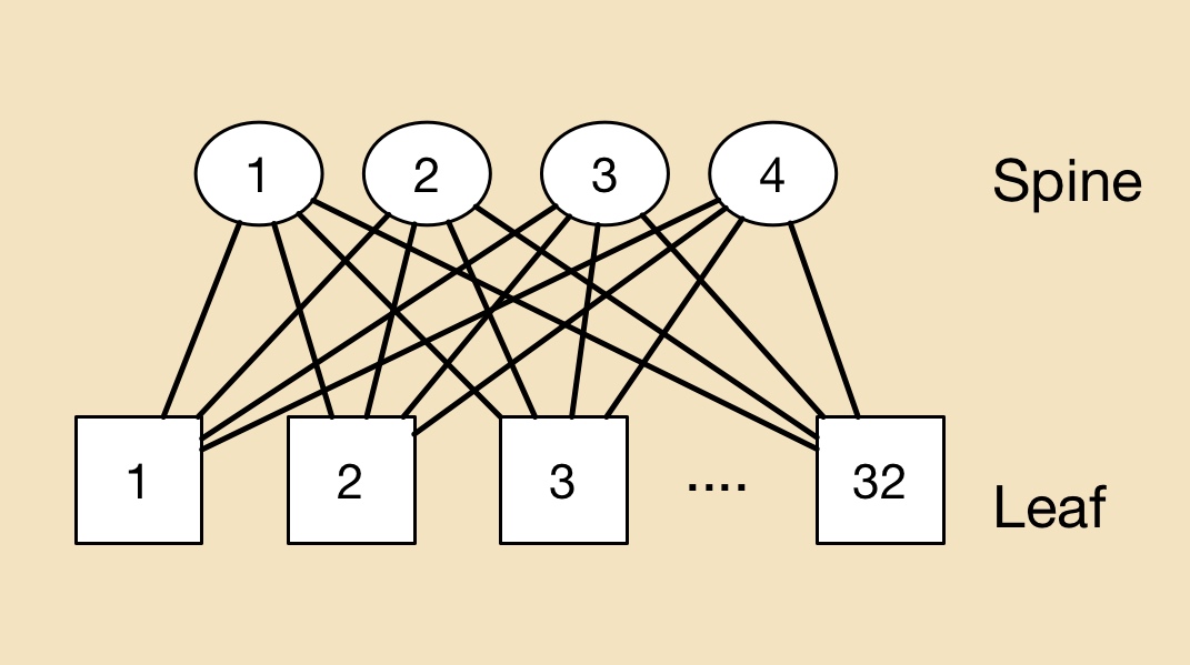
With the 4-port switch shown in Figure 1 it is assumed that each port can connect to the any of the other three ports. The 4-port switch is also non-blocking: if Port 1 is connected to Port 3, then the remaining input and output can also be used without affecting the link between ports 1 and 3. So, if four servers are connected to the ports, each can talk to any other server as shown in Figure 1.
 Figure 1: A 4-port switch. Source: Gazettabyte, Arista Networks
But once five or more servers need to be connected, things get more complicated. To double the size to create an 8-port switch, several 4-port basic building switches are needed, creating a more complex two-stage switching arrangement (Figure 2).
 Figure 2: An 8-port switch made up of 4-port switch building blocks. Source: Gazettabyte, Arista Networks.
Indeed the complexity increases non-linearly. Instead of one 4-port building block switch, six are needed for a switch with twice the number of ports, with a total of eight interconnections (number of second tier switches multiplied by the number of first tier switches).
Doubling the number of effective ports to create a 16-port switch and the complexity more than doubles again: now three tiers of switching is needed, 20 4-port switches and 32 interconnections (See Table 1).
 Table 1: How the number of 4-port building block switches and interconnects grow as the number of switch ports keep doubling. Source: Gazettabyte and Arista Networks.
The exponential growth in switches and interconnections is also plotted in Figure 3.
 Figure 3: The exponential growth in N-sized switches and interconnects as the switch size grows to 2N, 4N etc. In this example N=4. Source: Gazettabyte, Arista Networks.
This exponential growth in complexity explains Rockley Photonics’ goal to use silicon photonics to make a larger basic building block. Not only would this reduce the number of switches and tiers needed for the overall interconnection network but allow larger number of servers to be connected.
Rockley believes its silicon photonics-based switch will not only improve scaling but also reduce the size and power consumption of the overall interconnection network.
The start-up also claims that its silicon photonics switch will scale with Moore’s law, doubling its data capacity every two years. In contrast, the data capacity of existing switch ASICs do not scale with Moore’s law, it says. However the company has still to launch its product and has yet to discuss its design.
Data centre switching
In the data centre, a common switching arrangement used to interconnect servers is the leaf-and-spine architecture. A ‘leaf’ is typically a top-of-rack switch while the ‘spine’ is a larger capacity switch.
A top-of-rack switch typically uses 10 gigabit links to connect to the servers. The connection between the leaf and spine is typically a higher capacity link - 40 or 100 gigabit. A common arrangement is to adopt a 3:1 oversubscription - the total input capacity to the leaf switch is 3x that of its output stream.
To illustrate the point with numbers, a 640 gigabit top-of-rack switch is assumed, 480 gigabit (or 48 x10 Gig) capacity used to connect the servers and 160 gigabit (4 x 40 Gig) to link the top-of-rack switch to the spine switches.
In the example shown (Figure 4) there are 32 leaf and four spine switches connecting a total of 1,536 servers.
 Figure 4: An example to show the principles of a leaf and spine architecture in the data centre. Source: Gazettabyte
In a data centre with 100,000 servers, clearly a more complicated interconnection scheme involving multiple leaf and spine clusters is required.
Arista Network’s White Paper details data centre switching and leaf-and-spine arrangements, while Facebook published a blog (and video) discussing just how complex an interconnection network can be (see Figure 5).
 Figure 5: How multiple leaf and spines can be connected in a large scale data centre. Source: Facebook
Rockley demos a silicon photonics switch prototype
Rockley Photonics has made a prototype switch to help grow the number of servers that can be linked in a data centre. The issue with interconnection networks inside a data centre is that they do not scale linearly as more servers are added.
 Dr. Andrew Rickman
“If you double the number of servers connected in a mega data centre, you don’t just double the complexity of the network, it goes up exponentially,” explains Andrew Rickman, co-founder, chairman and CEO at Rockley Photonics. “That is the problem we are addressing.”
By 2017 and 2018, it will still be possible to build the networks that large-scale data centre network operators require, says Rickman, but at an ever increasing cost and with a growing power consumption. “The basic principles of what they are doing needs to be rethought,” he says.
Network scale
Modern data centre networks must handle significant traffic flow between servers, referred to as east-west traffic. A common switching arrangement in the data centre is the leaf-spine architecture, used to interconnect thousands of servers.
A ‘leaf’ may be a top-of-rack switch that is linked to multiple server chassis on one side and larger-capacity, ‘spine’ switches on the other. The result is a switch network where each leaf is connected to all the spine switches, while each spine switch is linked to all the leaves. In the example shown, four spine switches connect to 32 leaf switches.
 A leaf-spine architecture
The leaf and spine switches are built using ASICs, with the largest ICs typically having 32, 100 gigabit ports. One switch ASIC may be used in a platform but as Rickman points out, larger switches may implement multiple stages such as a three-stage Clos architecture. As a result, traffic between servers on different leaves, travelling up and down the leaf-spine, may pass through five stages or hops but possibly as many as nine.
There is no replacement performance in this area
It is the switch IC’s capacity and port count that dictates the overall size of the leaf-spine network and therefore the number of servers that can be connected. Rockley’s goal is to develop a bigger switch building block making use of silicon photonics.
“The fundamental thing to address is making bigger switching elements,” says Rickman. “That way you can keep the number of stages in the network the same but still make bigger and bigger networks.” Rockley expects its larger building-block switch will reduce the switch stages needed.
The UK start-up is not yet detailing its switch beyond saying it uses optical switching and that the company is developing a photonic integrated circuit (PIC) and a controlling ASIC.
“In the field of silicon photonics, for the same area of silicon, you can produce a larger switch; you have more capacity than you do in electronics,” says Rickman. Moreover, Rockley says that its silicon photonics-based PIC will scale with Moore’s law, with its switch's data capacity approximately doubling every two years. “Previously, the network did not scale with Moore’s law,” says Rickman.
Customers can see something is real and that it works. We are optimising all the elements of the system before taping out the fully integrated devices
Status
The company has developed a switch prototype that includes ‘silicon photonics elements’ and FPGAs. “Customers can see something is real and that it works,” says Rickman. “We are optimising all the elements of the system before taping out the fully integrated devices.” Rockley expects to have its switch in volume production in 2017.
Last year the company raised its first round of funding and said that it would undergo a further round in 2015. Rockley has not said how much it has raised or the status of the latest round. “We are well-funded and we have a very supportive group of investors,” says Rickman.
Rickman has long been involved in silicon photonics, starting out as a researcher at the University of Surrey developing silicon photonics waveguides in the early 1990s, before founding Bookham Technologies (now Oclaro). He has also been chairman of silicon photonics start-up Kotura that was acquired by Mellanox Technologies in 2013. Rickman co-founded Rockley in 2013.
“What I’ve learned about silicon photonics, and about all those electronics technologies, is how to design stuff from a process point of view to make something highly manufacturable and at the same time having the performance,” says Rickman.
There is no replacement performance in the area of data centre switching, he stresses: “The benefit of our technology is to deliver the performance, not the fact that it is cheap or [offers] average performance.”
For Part 2, Interconnection networks - an introduction, click here
Moore's law and silicon photonics
Chip pioneer Gordon E. Moore’s article appeared in the magazine Electronics in 1965. Dr. Moore was the director of the R&D labs at Fairchild Semiconductor, an early maker of transistors. Moore went on to co-found Intel, then a memory company, becoming its second CEO after Robert Noyce.
Moore’s article was written in the early days of integrated circuits. At the time, silicon wafers were one inch in diameter and integrating 50 components on a chip was deemed a state-of-the-art design.
Moore observed that, at any given time, there was an ideal number of components that achieved a minimum cost. Add a few more components and the balance would be tipped: the design would become overly complex, wafer yields would go down and costs would rise.
His key insight, later to become known as Moore’s law, was that integrated circuit complexity at this minimum cost was growing over time. Moore expected the complexity to double each year for at least another decade.
In his article he predicted that, by 1970, the manufacturing cost per component would be a tenth of the cost in 1965. Extrapolating the trend further, Moore believed that “by 1975, the number of components per integrated circuit for minimum cost will be 65,000 components.” Moore was overly optimistic, but only just: in 1975, Intel was developing a chip with 32,000 transistors.
“Perhaps we can say that the future of silicon photonics is the future of electronics itself.”
One decade after his article, Moore amended his law to a doubling of complexity every 24 months. By then the industry had started talking about transistors rather than components - circuit elements such as transistors, resistors and capacitors - after alighting on complementary metal oxide semiconductor (CMOS) technology to make the bulk of its chips. And in the years that followed, the period of complexity-doubling settled at every 18 months.
Moore has received less credit for his article's remarkable foresight regarding the importance of integrated circuits, especially when, in 1965, their merits were far from obvious. Such devices would bring a proliferation of electronics, he said, “pushing this science into many new areas”.
He foresaw home computers “or at least terminals connected to a central computer’, automatic control for automobiles and even mobile phones - ‘personal portable communications equipment’ as he called them. The biggest potential of ICs, he said, would be in the making of systems, with Moore highlighting computing, and telephone communications and switches.
The shrinking transistor
The shrinking of the transistor has continued ever since. And the technological and economic consequences have been extraordinary.
As a recent 50th anniversary Moore’s law article in IEEE Spectrum explains (link above), the cost of making a transistor in 1965 was $30 at today’s costs, in 2015 it is one billionth of a dollar. And in 2014, the semiconductor industry made 250 billion billion transistors, more transistors than had been made in all the years of the semiconductor industry up to 2011.
But the shrinking of the transistor cannot continue indefinitely, especially as certain transistor dimensions approach the atomic scale. As a result, many of the benefits that resulted with each shift to a new, smaller feature-sized CMOS process no longer hold.
To understand why, some understanding of CMOS and in particular, the MOS field effect transistor (MOSFET), is required.
Current flow between a MOSFET’s two terminals - the source and the drain - is controlled by a voltage placed on a third, electrical contact known as a gate. The gate comprises a thin layer of metal oxide, an oxide insulator on which sits a metal contact.
Several key dimensions define the MOSFET including the thickness of the oxide, the width of the source and the drain, and the gate length - the distance between the source and the drain.
Dennard scaling, named after IBM engineer and inventor of the DRAM, Robert Dennard, explains how the key dimensions of the transistor can all shrunk by the same factor, generation after generation. It is the effect of this scaling that makes Moore’s law work.
From the 1970s to the early 2000s, shrinking the transistor’s key dimension by a fixed factor returned a guaranteed bounty. More transistors could be placed on a chip allowing more on-chip integration, while each transistor became cheaper.
In turn, for a given chip area, the chip’s power density - the power consumption over a given area - remained constant. There may be more transistors crammed into a fixed area but the power each one consumes is less.
The predictable era of scaling transistors, after 50 years, is coming to an end and the industry is set to change
The transistor gate length feature size is used to define the CMOS technology or process node. In 1980, the minimum feature size was around 3 microns, nowadays CMOS chips typically use a 28 nanometer feature size - a 100 fold reduction. The metal oxide thickness has also been reduced one hundred times over the years.
But in the last decade Dennard scaling has come to an end.
The gate’s oxide thickness can no longer be trimmed as its dimensions are only a few atoms thick. The voltage threshold, the voltage applied to the gate to turn the transistor on, has also stopped shrinking, which in turn has stopped the scaling of the transistor’s upper voltage.
Why is this important? Because no longer being able to scale all these key parameters has meant that while smaller transistors can still be made, their switching speed is no longer increasing, nor is the power density constant.
Moreover, the very success of the relentless scaling means that the transistors are so tiny that new effects have come into play.
Transistors now leak current even when they are in the ‘off’ state. This means they consume power not only when they are being switched at high speed - the active power - but also they consume leakage power when they are off due to this current.
Process engineers now must work harder, to develop novel transistor designs and new materials to limit the leakage current. A second issue associated with the prolonged success of Dennard scaling is variability. Transistors are now less reliable and their performance less predictable.
The end of Dennard scaling means that the chip companies’ motivation to keep shrinking transistors is more to do with device cost rather than performance.
If, before, the power density stayed fixed with each new generation of CMOS process, more recently it has been the cost of manufacturing of a given area of silicon that has stayed fixed.
As the IEEE Spectrum Moore’s law article explains, this has been achieved by a lot of engineering ingenuity and investment. Device yield has gone up from 20 percent in the 1970s to between 80 and 90 percent today. The size of the silicon wafers on which the chips are made has also increased, from 8 inches to 12 inches. And while the lithography tools now cost one hundred-fold more than 35 years ago, they also pattern the large wafers one hundred times faster.
But now even the cost of making a transistor has stopped declining, according to The Linley Group, with the transition point being around the 28nm and 20nm CMOS.
Silicon manufacturing innovation will continue, and transistors will continue to shrink. Leading chip companies have 14nm CMOS while research work is now at a 7nm CMOS process. But not everyone will make use of the very latest processes, given how these transistors will be more costly.
Beyond Moore’s law
The industry continues to debate how many years Moore’s law still has. But whether Moore’s law has another 10 years or not, it largely does not matter.
Moore’s law has done its job and has brought the industry to a point where it can use billions of transistors for its chip designs.
But to keep expanding computing performance, new thinking will be required at many levels, spanning materials, components, circuit design, architectures and systems design.
The predictable era of scaling transistors, after 50 years, is coming to an end and the industry is set to change.
IBM announced last year its plan to invest US $3 billion over five years to extend chip development. Areas it is exploring include quantum computing, neurosynaptic computing, III-V technologies, carbon nanotubes, graphene, next-generation low-power transistors, and silicon photonics.
Silicon photonics
The mention of silicon photonics returns us to Gordon Moore’s 1965 article. The article starts with a bang: “The future of integrated electronics is the future of electronics itself".
Can the same be said of photonics?
Is the future of integrated photonics the future of photonics itself?
Daryl Inniss, vice president of Ovum’s components practice, argues this is certainly true. Photonics may not have one optical building block like electronics has the transistor, nor is there any equivalent of Dennard scaling whereby shrinking photonic functions delivers continual performance benefits.
But photonic integration does bring cost benefits, and developments in optical interconnect and long-haul transmission are requiring increasing degrees of integration, the sort of level of component integration associated with the chip industry at the time of Moore’s article.
And does the following statement hold true? “The future of silicon photonics is the future of photonics itself.”
“I think silicon photonics is bigger than photonics itself,” says Inniss. “Where do you draw the line between photonics and electronics? IBM, Intel and STMicroelectronics are all suppliers of electronics.”
Inniss argues that silicon photonics is an electronics technology. “Perhaps we can say that the future of silicon photonics is the future of electronics itself.”
Is silicon photonics an industry game-changer?
Briefing: Silicon Photonics
Part 3: Merits, challenges and applications
 Shown in blue are the optical waveguides (and bend radius) while the copper wires carrying high-speed electrical signals are shown in orange. Source: IBM
System vendors have been on a silicon-photonics spending spree.
Cisco Systems started the ball rolling in 2012 when it acquired silicon photonics start-up, LightWire, for $272M. Mellanox Technologies more recently bought Kotura for $82M. Now Huawei has acquired Caliopa, a four-year-old Belgium-based start-up, for an undisclosed fee. The Chinese system vendor has said it is looking to further bolster its European R&D, and highlighted silicon photonics in particular.
Given that it was only just over a decade ago when systems companies were shedding their optical component units, the trend to acquire silicon photonics highlights the growing importance of the fledgling technology.
These system vendors view silicon photonics as a strategic technology. The equipment makers want to develop expertise and experience as they plan to incorporate the technology in upcoming, hopefully differentiated platforms.
"If I have a Terabit of capacity on the front panel, how am I going to manipulate that across the line card, a fabric or the backplane?" says Adam Carter, general manager and senior director of the transceiver modules group at Cisco Systems. "We saw silicon photonics as a technology that could potentially enable us to get there."
System vendors are already using embedded optics - mounted on boards close to the ICs instead of pluggable modules on the front panel - to create platforms with denser interfaces.
"Photonics doesn't need the latest and greatest lithography"
Arista Networks' 7500E switch has a line card with board-mounted optics rather than pluggable transceivers to increase 100 Gigabit port density. The company offers several line cards using pluggable modules but it has designed one card with board-mounted optics that offers flexible interfaces - 10 Gig, 40 Gig and 100 Gig - and a higher port density. When developing the design, the multi-source agreement (MSA) CFP2 pluggable module was not ready, says Arista.
Compass-EOS, a core IP router start-up, has developed chip-mounted optics based on 168 lasers and 168 detectors. The novel Terabit-plus optical interface removes the need for a switch fabric and the mid-plane to interconnect the router card within the platform. The interface also enables linking of platforms to scale the IP core router.
Both companies are using VCSELs, an established laser technology that silicon photonics competes with. Yet the two designs highlight how moving optics closer to chips enables system innovation, a development that plays to silicon photonics' strength.
 "I characterise silicon photonics as a technology that will compete in the right applications but won’t displace indium phosphide" Ed Murphy, JDSU
Silicon photonics promises cost savings by enabling vendors to piggyback on the huge investments made by the semiconductor industry. Vendors making their own products, such as optical transceivers, also promises to shake up the existing optical component supply chain.
Cisco Systems' first silicon photonics product is the proprietary 100 Gigabit optical CPAK transceiver that is undergoing qualification. By making its own optical module, Cisco avoids paying the optical module makers' margins. Cisco claims the CPAK's smaller size improves the faceplate density compared to the CFP2.
Pros and cons
Silicon photonics may be able to exploit the huge investment already made in the semiconductor industry, but it does differ from standard CMOS integrated circuits (ICs).
First, optics does not have the equivalent of Moore's Law. Whereas chip economics improve with greater integration, only a few optical functions can be cascaded due to the accumulated signal loss as light travels through the photonic circuit. This is true for optical integration in general, not just silicon photonics.
Another issue is that the size of an optical component - a laser or a modulator - is dictated by the laws of physics rather than lithography. "Photonics doesn't need the latest and greatest lithography," says Martin Zirngibl, domain leader for enabling physical technologies at Alcatel-Lucent's Bell Labs. "You can live with 100nm, 120nm [CMOS] components whereas for electronics you want to have 45nm."
This can lead to the interesting situation when integrating electronics with photonics. "You either don't use the latest technology for electronics or you waste a lot of real estate with very expensive lithography for photonics," says Zirngibl.
Another disadvantage of silicon is that the material does not lase. As a result, either a III-V material needs to be bonded to the silicon wafer or an external laser must be coupled to the silicon photonics circuit.
Silicon also has relatively small waveguides which make it tricky to couple light in and out of a chip.
The advantages of silicon photonics, however, are significant.
The technology benefits from advanced 8- and 12-inch wafers and mature manufacturing processes developed by the semiconductor industry. Using such CMOS processes promises high yields, manufacturing scale, and automation and testing associated with large scale IC manufacturing.
"This is probably the only advantage but it is very significant," says Valery Tolstikhin, founder and former CTO of indium phosphide specialist, OneChip Photonics, and now an independent consultant. "It takes silicon totally off the scale compared to any other photonics materials."
"We can build the single-die optical engine in the same CMOS line where processors are built, where billions [of dollars] of investment has been done"
IBM's high-density silicon photonics optical engine is made using a 90nm CMOS process. "We can build the single-die optical engine in the same CMOS line where processors are built, where billions [of dollars] of investment has been done," says Yurii Vlasov, manager of the silicon nanophotonics department at IBM Research. "We are riding on top of that investment."
Extra processing may be introduced for the photonics, says IBM, but the point is that there is no additional capital investment. "It is the same tooling, the same process conditions; we are changing the way this tooling is used," says Vlasov. "We are changing the process a little bit; the capital investment is in place."
 "We believe that even for shorter distance, silicon photonics does compete in terms of cost with VCSELs." Yurii Vlasov, IBM
Stephen Krasulick, CEO of silicon photonics start-up, Skorpios Technologies, makes a similar point. "The real magic with our approach is the ability to integrate it with standard, commercial fabs," he says.
Skorpios is a proponent of heterogeneous integration, or what the company refers to as 'silicon photonics 2.0'. Here silicon and III-V are wafer-bonded and the optical components are created by etching the two materials. This avoids the need to couple external lasers and to use active alignment.
"We do it in a manner such that the CMOS foundry is comfortable letting the wafer back into the CMOS line," says Krasulick, who adds that Skorpios has been working with CMOS partners from the start to ensure that its approach suits their manufacturing flow.
Applications
The first applications adopting silicon photonics span datacom and telecom: from short-reach interconnect in the data centre to 100 Gigabit-per-second (Gbps) long-distance coherent transmission.
Intel is developing silicon photonics technology to help spur sales of its microprocessors. The chip giant is a member of Facebook's Open Compute Project based on a disaggregated system design that separates storage, computing and networking. "When I upgrade the microprocessors on the motherboard, I don't have to throw away the NICs [network interface controllers] and disc drives," says Victor Krutul, director business development and marketing for silicon photonics at Intel. The disaggregation can be within a rack or span rows of equipment.
"Optical modules do not require state-of-the-art lithography or large scale photonic integration, but they do need to be coupled in and out of fibre and they need lasers - none of that silicon photonics has a good solution for"
Intel has developed the Rack Scale Architecture (RSA) which implements a disaggregated design. One RSA implementation for Facebook uses three 100Gbps silicon photonics modules per tray. Each module comprises four transmit and four receive fibres, each at 25Gbps. Each tray uses a Corning-developed MXC connector and its ClearCurve fibre that support data rates up to 1.6Tbps. “Different versions of RSA will have more or less modules depending on requirements," says Krutul.
Luxtera, whose silicon photonics technology has been used for active optical cables, and Mellanox's Kotura, are each developing 100Gbps silicon photonics-based QSFPs to increase data centre reach and equipment face plate density.
One data centre requirement is the need for longer reach links. VCSEL technology is an established solution but at 100Gbps its reach is limited to 100m only. Intel's 100Gbps module, operating at 1310nm and combined with Corning's MXC connector and ClearCurve multi-mode fibre, enables up to 300m links. But for greater distances - 500m to 2,000m - a second technology is required. Data centre managers would like one technology that spans the data centre yet is cost competitive with VCSELs.
"Silicon photonics lends itself to that," says Cisco's Carter. "If we drive the cost lower, can we start looking at replacing or future proofing your network by going to single mode fibre?"
 "There are places where silicon photonics will definitely win, such as chip-to-chip optical interconnects, and there are places where there is still a question mark, like fibre-optics interconnects." Valery Tolstikhin
IBM's 25Gbps-per-channel optical engine has been designed for use within data centre equipment. "We are claiming we have density based on optical scaling which is the highest in the industry, and we have done it using monolithic integration: optical devices are built side-by-side with CMOS," says Vlasov.
What is important, says Vlasov, is not so much the size of the silicon waveguide but how sharp its bend radius is. The bend radius dictates how sharply the light can be guided while remaining confined within the integrated circuit. The higher the light confinement, the smaller the bend radius and hence the overall circuit area.
Much progress has been made in improving light confinement over the past two decades, resulting in the bend ratio coming down from 1cm to a micron. IBM claims that with its technology, it can build systems comprising hundreds of devices occupying a millimeter. "That is a major difference in the density of optical integration," says Vlasov.
IBM does not use heterogeneous integration but couples lasers externally."It is not complicated, it is a technical problem we are solving; we believe that is the way to go," says Vlasov. "The reason why we have gone down this path is very simple: we believe in monolithic integration where electrical circuitry sits side by side with optical components."
Such monolithic integration of the optics with the electronics, such as modulator drivers and clock recovery circuitry, reduces significantly the cost of packaging and testing. "We believe that even for shorter distances, silicon photonics does compete in terms of cost with VCSELs if all elements of the cost are taken care of: bill of materials, packaging and testing," says Vlasov.
But not everyone believes silicon photonics will replace VCSELs.
For example, Tolstikhin questions the merits of silicon photonics for transceiver designs, such as for 100 Gig modules in the data centre. "There are places where silicon photonics will definitely win, such as chip-to-chip optical interconnects, and there are places where there is still a question mark, like fibre-optics interconnects," he says.
Tolstikhin argues that silicon photonics offers little advantage for such applications: "Optical modules do not require state-of-the-art lithography or large scale photonic integration, but they do need to be coupled in and out of fibre and they need lasers - none of that silicon photonics has a good solution for."
Cisco says it was first attracted to LightWire's technology because of its suitability for optical transceivers. Six years ago 1W, SFP+ modules were limited to 10km. "Customers wanted 40km, 80km, even WDM," says Carter. "They [LightWire] did a 40km SFP+ using their modulator that consumed only 0.5W - a huge differentiator." Two years ago 100 Gig CFP modules were at 24W while LightWire demonstrated a module under 8W, says Carter.
Tolstikhin believes silicon photonics' great promise is for applications still to emerge. One example is chip-to-chip communication that has modest optical light requirements and does not have to be coupled in and out of fibre.
"Here you have very high requirements for density packaging and the tiny [silicon] waveguides are handy whereas indium phosphide is too big and too expensive here," says Tolstikhin. Longer term still, silicon photonics will be used for on-chip communication but that will likely be based on deep sub-wavelength scale optics such as surface plasmonics rather than classical dielectric waveguides.
Tolstikhin also argues that the economics of using indium phosphide compared to silicon photonics need not be all that gloomy.
Indium phosphide is associated with custom small-scale fabs and small volume markets. But indium phosphide can benefit from the economics of larger industries just as silicon photonics promises to do with the semiconductor industry.
Indium phosphide is used in higher volume for wireless ICs such as power amplifiers. "Quite significantly orders of magnitude higher," says Tolstikhin. The issue is that, conventionally, photonic circuits are fabricated by using multiple epitaxial growth steps, whereas the wireless ICs are made in a single-growth process, hence epitaxy and wafer processing are decoupled.
"If you can give up on regrowth and still preserve the desired photonic functionality, then you can go to commercial RF IC fabs," he says. "This is a huge change in the economic model." It is an approach that enables a fabless model for indium phosphide photonics, with the potential advantages not unlike those claimed by silicon photonics with respect to commercial CMOS fabs.
"That suggests indium phosphide - which has all kinds of physical advantages for those applications that require transmitters, receivers and fibre, plus readily available high-speed analogue electronics for trans-impedance amplifiers and laser or modulator drivers - may be quite a competitive contender," says Tolstikhin.
"Silicon photonics has a certain capability but the hype around it has magnified that capability beyond reality"
Customers don't care which technology is used inside a transceiver. "They care only about cost, power and package density," says Tolstikhin. "Indium phosphide can be competitive and on many occasions beat silicon photonics."
JDSU also believes that long-term, a perfect fit for silicon photonics may be relative short reach interconnects – chip-to-chip and board-to-board reaches. “You need to have very high speed and dense interconnects, I can see that as being a very strong value proposition long term," says Ed Murphy, senior director, communications and commercial optical products at JDSU.
Finisar and JDSU are open to the potential benefits of silicon photonics but remain strong proponents of traditional optical materials such as indium phosphide and gallium arsenide.
"We have designed silicon photonic chips here at Finisar and have evaluations that are ongoing. There are many companies that now offer silicon photonics foundry services. You can lay out a chip and they will build it for you," says Jerry Rawls, executive director of Finisar. "The problem is we haven't found a place where it can be as efficient or offer the performance as using traditional lasers and free-space optics."
"Silicon photonics has a certain capability but the hype around it has magnified that capability beyond reality,” says JDSU's Murphy. "Practitioners of silicon photonics would tell you that as well."
According to Murphy, each application, when looked at in detail, has its advantages and disadvantages when using either silicon photonics or indium phosphide. “Even in those applications where one or the other is better, the level of improvement is measured in a few tens of percent, not factors of ten,” he says. "I characterise silicon photonics as a technology that will compete in the right applications but won’t displace indium phosphide."
Silicon photonics for telecom
At the other extreme of the optical performance spectrum, silicon photonics is being developed for long-distance optical transmission. The technology promises to help shrink coherent designs to fit within the CFP2 module, albeit at the expense of reach. A CFP2 coherent module has extremely challenging cost, size and power requirements.
Teraxion is developing a coherent receiver for CFP2. "We believe silicon photonics is the material of choice to fulfill CFP2 requirements while allowing even smaller size reduction for future modules such as the CFP4," said Martin Guy, Teraxion's vice president of product management and technology.
u2t Photonics and Finisar recently licensed indium phosphide modulator technology to help shrink coherent designs into smaller form factor pluggables. So what benefit does silicon photonics offer here?
"In terms of size there will not be much difference between indium phosphide and silicon photonics technology," says Guy. "However, being on each side on the fence, we know that process repeatability and therefore yield is better with silicon photonics." Silicon photonics thus promises a lower chip cost.
"We have projects spanning everything from access all the way to long haul, and covering some datacom as well," says Rob Stone, vice president of marketing and program management at Skorpios. The start-up has developed a CMOS-based tunable laser with a narrow line width that is suitable for coherent applications.
"If you develop a library of macrocells, you can apply them to do different applications in a straightforward manner, provided all the individual macrocells are validated," says Stone. This is different to the traditional design approach.
Adding a local oscillator to a coherent receiver requires a redesign and a new gold box. "What we've got, we can plug things together, lay it out differently and put it on a mask," says Stone. "This enables us to do a lot of tailoring of designs really quite quickly - and a quick time-to-market is important."
Perhaps the real change silicon photonics brings is a disruption of the supply chain, says Zirngibl.
An optical component maker typically sells its device to a packaging company that puts it in a transmitter or receiver optical sub-assembly (TOSA/ ROSA). In turn, the sub-assemblies are sold to a module company which then sells the optical transceiver to an equipment vendor. Each player in the supply chain adds its own profit.
Silicon photonics promises to break the model. A system company can design its own chip using design tools and libraries and go to a silicon foundry. It could then go to a packaging company to make the module or package the device directly on a card, bypassing the module maker altogether.
Yet the ASIC model can also benefit module makers.
IBM has developed its 25Gbps-per-channel silicon photonics technology for its platforms, for chip-to-chip and backplanes, less for data centre interconnect. But it is open to selling the engine to interested optical module players. "If this technology can be extended to 2km for big data centres, others can come in, the usual providers of transceivers," says Vlasov.
"There are companies with the potential to offer a [silicon photonics] design service or foundry service to others that would like to access this technology," says Cisco's Carter. "Five years ago there wasn't such an ecosystem but it is developing very fast."
The article is an extended version of one that appeared in the exhibition magazine published at ECOC 2013.
Part 1: Optical interconnect, click here
Part 2: Bell Labs on silicon photonics, click here
Challenges, progress & uncertainties facing the optical component industry
In recent years the industry has moved from direct detection to coherent transmission and has alighted on a flexible ROADM architecture. The result is a new level in optical networking sophistication. OFC/NFOEC 2012 will showcase the progress in these and other areas of industry consensus as well as shining a spotlight on issues less clear.
Optical component players may be forgiven for the odd envious glance towards the semiconductor industry and its well-defined industry dynamics.
The semiconductor industry has Moore’s Law that drives technological progress and the economics of chip-making. It also experiences semiconductor cycles - regular industry corrections caused by overcapacity and excess inventory. The semiconductor industry certainly has its challenges but it is well drilled in what to expect.
Optical challenges
The optical industry experienced its own version of a semiconductor cycle in 2010-11 - strong growth in 2010 followed by a correction in 2011. But such market dynamics are irregular and optical has no Moore's Law.
Optical players must therefore work harder to develop components to meet the rapid traffic growth while achieving cost efficiencies, denser designs and power savings.
Such efficiencies are even more important as the marketplace becomes more complex due to changes in the industry layers above components. The added applications layer above networks was highlighted in the OFC/NFOEC 2012 news analysis by Ovum’s Karen Liu. The analyst also pointed out that operators’ revenues and capex growth rates are set to halve in the years till 2017 compared to 2006-2010.
Such is the challenging backdrop facing optical component players.
Consensus
Coherent has become the defacto standard for long-haul high-speed transmission. Optical system vendors have largely launched their 100Gbps systems and have set their design engineers on the next challenge: addressing designs for line rates beyond 100Gbps.
Infinera detailed its 500Gbps super-channel photonic integrated circuit last year. At OFC/NFOEC it will be interesting to learn how other equipment makers are tackling such designs and what activity and requests optical component vendors are seeing regarding the next line rates after 100Gbps.
Meanwhile new chip designs for transport and switching at 100Gbps are expected at the show. AppliedMicro is sampling its gearbox chip that supports 100 Gigabit Ethernet and OTU4 optical interfaces. More announcements should be expected regarding merchant 100Gbps digital signal processing ASIC designs.
An architectural consensus for wavelength-selective switches (WSSes) - the key building block of ROADMs - are taking shape with the industry consolidating on a route-and-select architecture, according to analysts.
Gridless - the ROADM attribute that supports differing spectral widths expected for line rates above 100Gbps - is a key characteristic that WSSes must support, resulting in more vendors announcing liquid crystal on silicon designs.
Client-side 40 and 100 Gigabit Ethernet (GbE) interfaces have a clearer module roadmap than line-side transmission. After the CFP comes the CFP2 and CFP4 which promise denser interfaces and Terabit capacity blades. Module form factors such as the QSFP+ at 40GbE and in time 100GbE CFP4s require integrated photonic designs. This is a development to watch for at the show.
Others areas to note include tunable-laser XFPs and even tunable SFP+, work on which has already been announced by JDS Uniphase.
Lastly, short-link interfaces and in particular optical engines is another important segment that ultimately promises new system designs and the market opportunity that will unleash silicon photonics.
Optical engines can simplify high-speed backplane designs and printed circuit board electronics. Electrical interfaces moving to 25Gbps is seen as the threshold trigger when switch makers decide whether to move their next designs to an optical backplane.
The Optical Internetworking Forum will have a Physical and Link Layer (PLL) demonstration to showcase interoperability of the Forum’s Common Electrical Interface (CEI) 28Gbps Very Short Reach (VSR) chip-to-module electrical interfaces, as well as a demonstration of the CEI-25G-LR backplane interface.
Companies participating in the interop include Altera, Amphenol, Fujitsu Optical Components, Gennum, IBM, Inphi, Luxtera, Molex, TE Connectivity and Xilinx.
Altera has already unveiled a FGPA prototype that co-packages 12x10Gbps transmitter and receiver optical engines alongside its FPGA.
Uncertainties
OFC/NFOEC 2012 also provides an opportunity to assess progress in sectors and technology where there is less clarity. Two sectors of note are next-generation PON and the 100Gbps direct-detect market.
For next-generation PON, several ideas are being pursued, faster extensions of existing PON schemes such as a 40Gbps version of the existing time devision multiplexing PON schemes, 40G PON based on hybrid WDM and TDM schemes, WDM-PON and even ultra dense WDM-PON and OFDM-based PON schemes.
The upcoming show will not answer what the likely schemes will be but will provide an opportunity to test what the latest thinking is.
The same applies for 100 Gigabit direct detection.
There are significant cost advantages to this approach and there is an opportunity for the technology in the metro and for data centre connectivity. But so far announcements have been limited and operators are still to fully assess the technology. Further announcements at OFC/NFOEC will highlight the progress being made here.
The article has been written as a news analysis published by the organisers before this year's OFC/NFOEC event.