Nubis' bandwidth-packed tiny optical engine
- Nubis Communications has revealed its ambitions to be an optical input-output (I/O) solutions provider
- Its tiny 1.6-terabit optical engine measures 5mm x 7.5mm
- The optical engine has a power consumption of below 4 picojoule/bit (pJ/b) and a bandwidth density of 0.5 terabits per millimetre.
- “Future systems will be I/O with an ASIC dangling off it.”
Nubis Communications has ended its period of secrecy to unveil an optical engine targeted at systems with demanding data input-output requirements.
The start-up claims its optical engine delivers unmatched bandwidth density measured in terabits per millimetre (T/mm) and power consumption performance metrics.
“In the timeframe of founding the company [in 2020], it became obvious that the solution space [for our product] was machine learning-artificial intelligence,” says Dan Harding, the CEO of Nubis.
Company Background
Nubis has raised over $40 million, with the lead investor being Matrix Partners. Venture capital company Matrix Partners backed Acacia Communications, acquired by Cisco in 2021.
Other Nubis backers are Weili Dai, a co-founder of Marvell Technologies, and Belgium-based imec.xpand.

“We have raised enough money to get to production with our product,” says Harding, who joined Nubis in 2021 from Broadcom.
Peter Winzer is the CTO and founder of the company. Formerly at Nokia Bell Labs, Winzer was the 2018 winner of the Optica (then OSA) and IEEE Photonics Society’s John Tyndall Award for his work on coherent optical communications.
Nubis has 40 staff, mostly engineers.
“As a team, we are multidisciplinary,” says Winzer. The company’s expertise includes silicon photonics, analogue IC design including serialisers/ deserialisers (serdes), packaging – electrical and optical, and software including advanced simulation tools.
“It is all geared towards a systems solution,” says Winzer. “We are not just looking at the PIC [photonic integrated circuit] or the electronics; we have the system and the architecture in mind.”
The input-output challenge
Machine learning workloads continue to grow at a staggering pace, doubling more than twice each year. Not surprisingly, computing systems running such workloads are struggling to keep up.
Scaling such systems not only requires more processing – more graphics processing units (GPUs) – but also networking to connect clusters of GPUs.
What the compute vendors want is any-to-any connectivity between processors and between clusters. This is creating a tremendous input-output challenge in terms of bandwidth density while keeping the power consumption under control.
“Over half the power of that cluster can be taken up by traditional optics,” says Harding. “So it is clear that the industry wants new solutions.”
“Whatever cents-per-gigabit [figure] you use, if you multiply it by the I/O capacity, the number you’ll get is many times that of [the cost of] an ASIC,” adds Winzer. “We say that future systems will be I/O with an ASIC dangling off it.”

Design details
Nubis’ optical engine is a 16 x 112-gigabit design with a footprint of 5mm x 7.5mm.
“Because we have our electronics flip-chipped on top, that’s the entire footprint,” says Winzer. “We maintain that it is the highest density by far of any optical engine.”
Nubis says many parallel fibres can be interfaced to the optical engine despite its tiny size.
Supporting parallel fibres is essential for machine learning systems as the fibres are fanned out to enable any-to-any connectivity.
Nubis’ engine uses a 4 by DR4 fan-out architecture with 36 fibres arranged in a 3×12 array.
Surface coupling in a 2D array interfaces the 36 fibres to the PIC: 32 fibres are for data and four for the external laser light source.
There is only a physical limit to the number of fibres that can be connected if edge coupling is used, says Winzer. But surface coupling in a 2D array means the optical engine delivers 5-10x more density than its competitors.
The start-up also has designed the engine’s electronics: the optical modulator driver and the trans-impedance amplifier (TIA). The electronics use advanced equalisation to boost the electrical channel, given direct drive has demanding requirements, says Harding.
The XT1600 optical module
Nubis’ first product is the XT1600 optical module. Here, a substrate houses the company’s PIC and electronics onto which is packaged a lid containing the optical fibres.
Nubis has developed in-house the packaging and the fibre attach solution.
The substrate is 15x15mm, somewhat larger than the engine. Harding says this is deliberate to support products under development.
The 1.6 terabits – in fact, 16x112Gbps full duplex – module has a 2km reach. Its power consumption is below 4 pJ/b.
The fibres exit the module vertically and bend to the side. “[Going] vertical is good but the 2D is the much more important aspect here,” says Winzer.
A 2D approach is logical, says Nubis. An electrical ball grid array (BGA) all the bottom surface. It makes sense that the optics is similarly massively 2D, especially for designs where its a 100-gigabit electrical signal in and a 100-gigabit optical signal out.
Multiple rings of optical I/O engines can surround the ASIC because the fibres exit vertically. “Nobody else can do that because they are escaping from the [PIC] edge,” says Winzer.
Winzer highlights another benefit of the design.
The Universal Chiplet Interconnect Express (UCIe) specification calls for 2T/mm bandwidth escape density. An optical chiplet can only achieve this if wavelength-division multiplexing (WDM) is used due to the large fibre size. Nubis can achieve this density optically without having to use WDM because of 2D surface coupling.
Doing all-to-all at scale remains a big system challenge. “We’re just a part of that challenge,” says Harding. But for optical I/O to become pervasive in the data centre over the next five years, the optics must be significantly lower power, smaller, and efficient.
“If you crack that 2D nut, you can do many, many great things down the road,” says Winzer. “We’ve solved a huge technology problem that allows us to scale much better than anybody else.”
Status
Nubis has not named its foundry and contract manufacturing partners but says they are large, high-volume manufacturers.
Harding says there are now up to five credible silicon photonic foundries available.
“There was some early product definition which some foundries were better suited to support,“ says Harding. “And there was a robustness of the initial PDKs [process design kits] to get us an early product that was important to us.”
Choosing a contract manufacturer proved easier, given the maturity of the players.
Nubis’ first product has 16 optical channels each at 112 gigabit, but future designs will offer N by 224-gigabit channels.
Meanwhile, the XT1600 optical engine is available for sampling.
OFC 2023 show preview
- Sunday, March 5 marks the start of the Optical Fiber Communication (OFC) conference in San Diego, California
- The three General Chairs – Ramon Casellas, Chris Cole, and Ming-Jun Li – discuss the upcoming conference
OFC 2023 will be a show of multiple themes. That, at least, is the view of the team overseeing and coordinating this year’s conference and exhibition.
General Chair Ming-Jun Li of Corning who is also the recipient of the 2023 John Tyndall Award (see profiles, bottom), begins by highlighting the 1,000 paper submissions, suggesting that OFC has returned to pre-pandemic levels.
Ramon Casellas, another General Chair, highlights this year’s emphasis on the social aspects of technology. “We are trying not to forget what we are doing and why we are doing it,” he says.
Casellas highlights the OFC’s Plenary Session speakers (see section, below), an invited talk by Professor Dimitra Simeonidou of the University of Bristol, entitled: Human-Centric Networking and the Road to 6G, and a special event on sustainability.
This year’s OFC has received more submissions on quantum communications totaling 66 papers.
In the past, papers on quantum communications were submitted across OFC’s tracks addressing networking, subsystems and systems, and devices. However, evaluating them was challenging given that only some reviewers are quantum experts, says Chris Cole, the third General Chair. Now, OFC has a subcommittee dedicated to quantum.
Another first is OFCnet, a production network that will run during the show.
Themes and topics
Machine learning is one notable topic this year. The subject is familiar at OFC, says Casellas, but people are discussing it more.
Casellas highlights one session at OFC 2021 that addressed machine learning for optics and optics for machine learning. “It showed the duality of how you can use photonic components to do machine learning and apply machine learning to optimise networking,” says Casellas.
This year there will be additional aspects of machine learning for networks, transmission, and operations, says Casellas.
Other General Chair highlighted subjects include point-to-multipoint coherent transmission, non-terrestrial and satellite networks, and optical switching and how its benefits networking in the data centre.
Google, for example, is presenting a paper detailing its use of optical switching in its data centres, something the hyperscaler disclosed at the ACM Sigcomm conference in August 2022.
There is also more interest in fibre sensors used in communications networks.
“We see an increasing trend because now if you want smart networks, you need sensors everywhere,” says Li.
“That is another theme that goes across all the tracks, which is a non-traditional optical fibre communication area that we’ve been embracing,” adds Cole.
As examples, Cole cites lidar, radio over fibre, free-space communications, microwave fibre sensing, and optical processing.
OFC has had contributions in these areas, he says, but now these topics have dedicated subcommittee titles.
Plenary session
This year’s three Plenary Session speakers are:
- Patricia Obo-Nai, CEO of Vodafone Ghana, who will discuss Harnessing Digitalization for Effective Social Change,
- Jayshree V. Ullal, president and CEO of Arista Networks, addressing The Road to Petascale Cloud Networking,
- and Wendell P. Weeks, chairman and CEO of Corning, whose talk is entitled Capacity to Transform.
“We thought that having someone who could explain how technology improves society would be very positive,” says Casellas. “I’m proud to have someone who can talk on the benefits of digitisation from the point of view of society, in addition to more technical topics.”
Li highlights how OFC celebrated the 50th anniversary of low-loss fibre two years ago and that last year, OFC celebrated the year of glass, displaying information on panels.
Corning has played an important role in both technologies. “Having a speaker [Wendell Weeks] from a glass company talking about both will be interesting to the OFC audience,” says Li.
Cole highlights the third speaker, Jayshree Ullal, the CEO of Arista. The successful networking player is one of the companies competing in what he describes as a very tough field.
Rump session
This year’s Rump Session tackles silicon photonics, a session moderated by Daniel Kuchta of IBM TJ Watson Research Center and Michael Hochberg of Luminous Computing.
Cole says silicon photonics has received tremendous attention, and the Rump Session is asking some tough questions: “Is silicon photonics for real now? Is it just one of the guys in the toolbox? Or is it being sunsetted or supplemented?”
Cole expects a lively session, not just challenging conventional thinking but having people representing exciting alternatives which are commercially successful alongside silicon photonics.
Show interests
The Chairs also highlight their interests and what they hope to learn from the show.
For Li, it is high-density fibre and cable trends.
Work on space division multiplexing (SDM) – multicore and multimode – fibre has been an OFC topic for over 15 years. One question Li has is whether systems will use SDM.
“It looks like multicore fibre is close, but we want to learn more from customers,” says Li.
Another interest is an alternative development of reduced coating diameter fibres that promise greater cable density. “I always think this is probably the short-term solution, but we’ll see what people think,” says Li.
AI drives interest in fibre density and latency issues in the data centre. Low latency is attracting interest in hollow-core fibre. Microsoft acquired Lumenisity, a UK hollow core fibre specialist, late last year.
Li is keen to learn more about quantum communications. “We want to understand, from a fibre component point of view, what to do in this area.”
Until now industry focus has been on quantum key distribution (QKD), but Li wants to learn about other applications of quantum in telecoms.
The bandwidth challenge facing datacom is Cole’s interest.
As the Rump Session shows, there has been an explosion of technologies to address data challenges, particularly in the data centre. “So I’m looking forward to continuing to see all the great ideas and all the different directions,” says Cole.
Another show interest for Cole is start-ups in components, subsystems and systems, and networking.
At Optica’s Executive Forum, held on Monday, March 6, a session is dedicated to start-ups. Casellas is looking forward to the talks on optical network automation.
Much work has applied machine learning to optical transmission and amplifier optimisation. Casellas wants to see how reinforcement learning is applied to optical network controllers. Telemetry and its use for network monitoring are another of his interests.
“Maybe because I’m an academic and idealistic, but I like everything related to disaggregation and the opening of interfaces,” says Casellas, who too wants to learn more about quantum.
“I have a basic understanding of this, but maybe it is hard to get into something new,” says Casellas. Non-terrestrial and satellite networks are other topics of interest.
Cole concludes with a big-picture view of photonics.
“It’s a great time to be in optics,” he says. “We’re seeing an explosion of creativity in different areas to solve problems.”
Ramon Casellas works at the Centre Tecnològic de Telecomunicacions de Catalunya (CTTC) research institution in Barcelona, Spain. His research focuses on networks – particularly the control plane, operations and management – rather than optical systems and devices.
Ming-Jun Li is a Corporate Fellow at Corning where he has that worked for 32 years.
Li is also this year’s winner of the John Tyndall Award, presented by Optica and the IEEE Photonics Society. The award is for Li’s ‘seminal contributions to advances in optical fibre technology.’
“It was a surprise to me and a great honour,” says Li. “The work is not only for myself but for many people working with me at Corning; I cannot achieve without working with meaningful colleagues.”
Chris Cole is a consultant whose background is in datacom optics. He will be representing the company, Coherent, at OFC.

Waiting for buses: PCI Express 6.0 to arrive on time

- PCI Express 6.0 (PCIe 6.0) continues the trend of doubling the speed of the point-to-point bus every 3 years.
- PCIe 6.0 uses PAM-4 signalling for the first time to achieve 64 giga-transfers per second (GT/s).
- Given the importance of the bus for interconnect standards such as the Compute Express Link (CXL) that supports disaggregation, the new bus can’t come fast enough for server vendors.
The PCI Express 6.0 specification is expected to be completed early next year.
So says Richard Solomon, vice-chair of the PCI Special Interest Group (PCI-SIG) which oversees the long-established PCI Express (PCIe) standard, and that has nearly 900 member companies.
The first announced products will then follow later next year while IP blocks supporting the 6.0 standard exist now.
When the work to develop the point-to-point communications standard was announced in 2019, developing lanes capable of 64 giga transfers-per-second (GT/s) in just two years was deemed ambitious, especially given 4-level pulse amplitude modulation (PAM-4) would be adopted for the first time.
But Solomon says the global pandemic may have benefitted development due to engineers working from home and spending more time on the standard. Demand from applications such as storage and artificial intelligence (AI)/ machine learning have also been driving factors.
Applications
The PCIe standard uses a dual simplex scheme – serial transmissions in both directions – referred to as a lane. The bus can be configured in several lane configurations: x1, x2, x4, x8, x12, x16 and x32, although x2, x12 and x32 are rarely used in practice.
PCIe 6.0’s transfer rate of 64GT/s is double that of the PCIe 5.0 standard that is already being adopted in products.
The PCIe bus is used for storage, processors, AI, the Internet of Things (IoT), mobile, and automotive especially with the advent of advanced driver assistance systems (ADAS). “Advanced driver assistance systems use a lot of AI; there is a huge amount of vision processing going on,” says Solomon.
For cloud applications, the bus is used for servers and storage. For servers, PCIe has been adopted by general-purpose processors and more specialist devices such as FPGAs, graphics processor units (GPUs) and AI hardware.
IBM’s latest 7nm POWER10 16-core processor, for example, is an 18-billion transistor device. The chip uses the PCIe 5.0 bus as part of its input-output.
In contrast, IoT applications typically adopt older generation PCIe interfaces. “It will be PCIe at 8 gigabit when the industry is on 16 and 32 gigabit,” says Solomon.
PCIe is being used for IoT because of it being a widely adopted interface and because PCIe devices interface like memory, using a load-store approach.
The CXL standard – an important technology for the data centre that interconnects processors, accelerator devices, memory, and switching – also makes use of PCIe, sitting on top of the PCIe physical layer.

PCIe roadmap
The PCIe 4.0 came out relatively late but then PCI-SIG quickly followed with PCIe 5.0 and now the 6.0 specification.
The PCIe 6.0 specification built into the schedule an allowance for some slippage while still being ready for when the industry would need the technology. But even with the adoption of PAM-4, the standard has kept to the original ambitious schedule.
PCIe 4.0 incorporated an important change by extending the number of outstanding commands and data. Before the 4.0 specification, PCIe allowed for up to 256 commands to be outstanding. With PCIe 4.0 that was tripled to 768.
To understand why this is needed, a host CPU system may support several add-in cards. When a card makes a read request, it may take the host a while to service the request, especially if the memory system is remote.
A way around that is for the add-in card to issue more commands to hide the latency.
“As the bus goes faster and faster, the transfer time goes down and the systems are frankly busier,” says Solomon. “If you are busy, I need to give you more commands so I can cover that latency.”
The PCIe technical terms are tags, a tag identifying each command, and credits which refers to how the bus takes care of flow control.
“You can think of tags as the sheer number of outstanding commands and credits as more as the amount of overall outstanding data,” says Solomon.
Both tags and credits had to be changed to support up to 768 outstanding commands. And this protocol change has been carried over into PCI 5.0.
In addition to the doubling in transfer rate to 32GT/s, PCI 5.0 requires an enhanced link budget of 36dB, up from 28dB with the PCIe 4.0. “As the frequency [of the signals] goes up, so does the loss,” says Solomon.
PCI 6.0
Moving from 32GT/s to 64GT/s and yet keep ensuring the same typical distances requires PAM-4.
More sophisticated circuitry at each end of the link is needed as well as a forward-error correction scheme which is a first for a PCI express standard implementation.
One advantage is that PAM-4 is already widely used for 56 and 112 gigabit-per-second high-speed interfaces. “That is why it was reasonable to set an aggressive timescale because we are leveraging a technology that is out there,” says Solomon. Here, PAM-4 will be operated at 64Gbps.
The tags and credits have again been expanded for PCI 6.0 to support 16,384 outstanding commands. “Hopefully, it will not be needed to be extended again,” says Solomon.
PCIe 6.0 also supports FLITs – a network packet scheme – that simplifies data transfers. FLITs are introduced with PCIe 6.0, but silicon designed for PCIe 6.0 could use FLITs at lower transfer speeds. Meanwhile, there are no signs of PCI Express needing to embrace optics as the interface speeds continue to advance.
“There is a ton of complexity and additional stuff we have to do to move to 6.0; optical would add to that,” says Solomon. “As long as people can do it on copper, they will keep doing it on copper.”
PCI-SIG is not yet talking about PCIe 7.0 but Solomon points out that every generation has doubled the transfer rate.
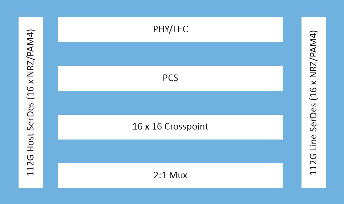
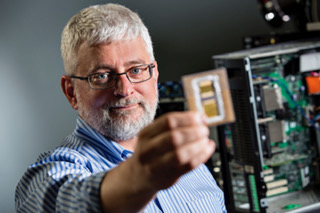
Microchip’s compact, low-power 1.6-terabit PHY

Microchip Technology’s latest physical layer (PHY) chip has been developed for next-generation line cards.
The PM6200 Meta-DX2L (the ‘L’ is for light) 1.6-terabit chip is implemented using TSMC’s 6nm CMOS process. It is Microchip’s first PHY to use 112-gigabit PAM-4 (4-level pulse-amplitude modulation) serialiser/ deserialisers (serdes) interfaces.
Microchip’s existing 16nm CMOS Meta-DX1 PHY devices are rated at 1.2 terabits and use 56-gigabit PAM-4 serdes.
System vendors developing line cards that double the capacity of their switch, router or transport systems are being challenged by space and power constraints, says Microchip. To this aim, the company has streamlined the Meta-DX2L to create a compact, lower-power chip.
“One of the things we have focussed on is the overall footprint of our [IC] design to ensure that people can realise their cards as they go to the 112-gigabit PAM-4 generation,” says Stephen Docking, manager, product marketing, communications business unit, at Microchip.
The company says the resulting package measures 23x30mm and reduces the power per port by 35 per cent compared to the Meta-DX1.
IC architecture
The Meta-DX1 family of 1.2-terabit physical layer (PHY) Ethernet chips effectively comprise three 400-gigabit cores and support the OIF’s Flexible Ethernet (FlexE) protocol and MACsec encryption.
The Meta-DX1 devices, launched in 2019, support the Precision Time Protocol (PTP) used to synchronise clocks across a network with high accuracy that is a requirement for 5G.
The new Meta-DX2L is a single chip although Microchip hints that other family devices will follow.
The Meta-DX2L can be viewed as comprising two 800-gigabit cores. The chip does away with FlexE and the PTP protocol but includes retiming and gearbox modes. The gearbox is used to translate between 28, 56 and 112-gigabit rates.
“We still see customers working on FlexE designs, so the lack of it [with the Meta-DX2L] is not due to limited market demand but how we chose to optimise the chip,” says Docking.
The same applies to PTP. The Meta-DX1 performs time stamping that meets 5G’s Class C and Class D front-haul clocking requirements. “The difference with the Meta-DX2L is that it is not doing time stamping,” says Docking. But it can work with devices doing the time stamping.
“In a 5G system, if you add a PHY, you need to do it in such a way that it doesn’t add any uncertainty in the overall latency of the system,” says Docking. ”So we have focussed on the device have a constant latency.” This means the Meta-DX2L can be used in systems meeting Class C or Class D clocking requirements.
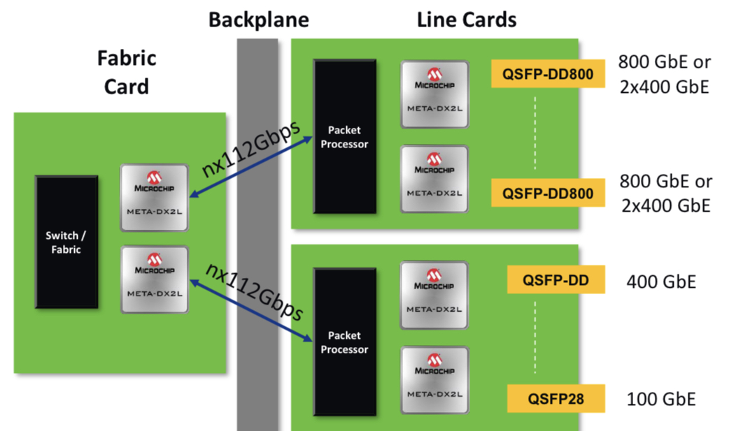
The chip also features a 16×16 crosspoint switch that allows customers to use different types of optical modules and interface them to a line card’s ASIC or digital signal processor (DSP).
The Meta-DX2L’s two cores are flexible and support rates from 1 to 800 Gigabit Ethernet, says Docking.
As well as Ethernet rates, the device supports proprietary rates common with artificial intelligence (AI) and machine learning.
For AI, an array of graphic processor units (GPUs) talk to each other on the same line card. “But to scale the system, you have to have multiple line cards talk to each other,” says Docking. “Different companies that design GPUs have chosen their own protocols to optimise their communications.”
Such links are not aligned with the Ethernet rates but the Meta-DX2L supports these proprietary rates.
Microchip says the Meta-DX2L will sample this quarter.
1.6 terabits, system resilience and design challenges
The PHY’s 1.6-terabit capacity was chosen based on customers’ requirements.
“If you look at the number of ports people want to support, it is often an even multiple of 800-gigabit ports,” says Docking.
The Meta-DX2L, like its predecessor PHY family, has a hitless 2:1 multiplexer. The multiplexer function is suited for centralised switch platforms where the system intelligence resides on a central card while the connecting line cards are relatively simple, typically comprising PHYs and optical modules.
In such systems, due to the central role of the platform’s switch card, a spare card is included. Should the primary card fail, the backup card kicks in, whereby all the switch’s line cards connect to the backup. The 2:1 multiplexer in the PHY means each line card is interfaced to both switch cards: the primary one and backup.

For line cards that will have 32 or 36 QSFP-DD800 pluggable modules, space is a huge challenge, says Docking: “So having a compact PHY is important.”
“The physical form factor has always been a challenge and then density plays into it and thermal issues,” says Kevin So, associate director, product line management and marketing, communications business unit, at Microchip. “And when you overlay the complexity of the transition from 56 to 112 gigabits, that makes it extremely challenging for board designers.”
Applications
The 1.6-terabit PHY is aimed at switching and routing platforms, compact data centre interconnect systems, optical transport and AI designs.
Which application takes off first depends on several developments. On one side of the PHY chip sits the optics and on the other the ASIC, whether a packet processor, switch chip, processor or DSP. “It’s the timing of those pieces that drive what applications you will see first,” says So.
“Switching and packet processor chips are transitioning to 112-gigabit serdes and you are also starting to see QSFP-DD or OSFP optics with 112-gigabit serdes becoming available,” adds Docking. “So the ecosystem is starting for those types of systems.”
The device is also being aimed at routers for 5G backhaul applications. Here data rates are in the 10- to the 100-gigabit range. “But you are already starting to hear about 400-gigabit rates for some of these access backhaul routers,” says So.
And with 400 Gigabit Ethernet being introduced on access pizza-box routers for 5G this year, in two years, when Microchip’s customers release their hardware, there will likely be denser versions, says So.
“And by then we’ll be talking about a DX3, who knows?” quips So.

Making optical networking feel like cycling downhill

BT’s chief architect, Neil McRae, is a fervent believer in the internet, a technology built on the continual progress of optical networking. He discussed both topics during his invited talk at the recent OFC 2021 virtual conference and exhibition.
Neil McRae’s advocacy of the internet as an educational tool for individuals from disadvantaged backgrounds stems from his childhood experiences.
“When I was a kid, I lived in a deprived area and the only thing that I could do was go to the library,” says McRae, chief architect and managing director for architecture and technology strategy at BT.
His first thought on discovering the internet was just how much there was to read.
“If I’m honest, everything I’ve learnt in technology has been pretty much self-taught,” says McRae.
This is why he so values the internet. It has given him a career where he has travelled widely and worked with talented and creative people.
“Anyone who is out there in the world can do the same thing,” he says. “I strongly believe that the internet brings opportunities to people who are willing to spend the time to learn.”
Optical networking
McRae surveyed the last 20 years of optical networking in his OFC talk. He chose the period since it was only at the end of the last century that the internet started to have a global impact.
“The investment in networking [during this period] has been orders of magnitude bigger than prior years,” says McRae. “There has also been a lot of deregulation across the world, more telecoms companies, more vendors and ultimately more people getting connected.”
In 2000, networks used the SONET/SDH protocol and fixed wavelengths. “We have brought in many new technologies – coherent, coloured optics, programable lasers and silicon photonics – and they have been responsible for pretty significant changes.”
McRae likens optical network to gears on a bike. “It powers the rest of what we do in the network and without those advances, we wouldn’t be the digitally connected society we are today,” says McRae. “If I think about the pandemic of the last year, can you imagine what the pandemic would have been like if it had happened in the year 2000?”
McRae says he spends a fifth of his time on optical networking. This is more than previously due to the relentless growth in network bandwidth.
“Ultimately, if you get optical wrong, it feels like you are in the wrong gear cycling uphill,” says McRae. “If you get it right, you are in the right gear, you are going as fast as you can go and it feels like a downhill ride.”
And it’s not just bandwidth but also from a cost, capability and customer experience perspective. “We recognise the value that it brings to all the other layers right up to the application,” he says.
Research
BT Labs has an optical networking programme that is run by Professor Andrew Lord. The programme’s remit is to help BT address existing and future issues.
“There is a longer-term research aspect to what Andrew and his team do, but there are some here-and-now issues that they support me on like the hollow-core fibre work and some of the 400-gigabit [coherent] platforms we have been reviewing recently,” he says.
He cites as examples the work the programme did for BT’s next-generation optical platform that was designed for growth and which indeed has grown massively in the last decade. “We have launched optical services as a product because of the platform,” says McRae.
The programme has also helped Openreach, BT Group’s copper and fibre plant subsidiary, with its fibre-to-the-premise (FTTP) deployments that use such technologies as GPON and XGS-PON.
Reliable, dynamic, secure networks
McRae admits he is always nervous about predicting the future. But he is confident 400 gigabits will be a significant optical development over the next decade.
This includes inside the data centre, driven by servers, and in the network including long haul.
“The challenge will be around getting the volume and interoperability as quickly as we possibly can,” says McRae.
The other big opportunity is the increased integration of IP and optical using a control plane aligned to both.
“The biggest networking technology out there is IP,” says McRae. “And that will not change in the coming decade.”
The Layer-3 capabilities include working around issues but it is bad at managing bandwidth. Optical is the opposite: great at managing bandwidth but less dynamic for working around problems. Merging the two promises significant benefits.
This idea, advocated as IP-over-DWDM, has long been spoken of but has not been deployed widely. The advent of 400-gigabit coherent implemented using client-side modules means that the line-side interface density can equal that of the host. And other developments such as software-defined networking and artificial intelligence also help.
Software-defined networking will make a big difference because it will enable the move to automation and that will enable new technologies such as artificial networking (AI) and machine-learning to be introduced.
McRae talks of a control plane capable of deciding which interface to send packets down and also determine what paths to create across the optical infrastructure.
“We have seen some of that but we have not seen enough,” says McRae. AI and machine-learning technologies will provide networks with almost autonomous control over which paths to use and enable for the various traffic types the network sees.
McRae stresses that it is getting harder to get the maximum out of the network: “If we maintain human intervention, the network will never see its full potential because of complexity, demands and scale.”
He predicts that once the human component is taken out of the network, some of the silos between the different layers will be removed. Indeed, he believes networks built by AI and aided by automation will look very different to today’s networks.
Another technology McRae highlights is hollow-core fibre which BT Labs has been researching.
“Increasingly, we are starting to reach some limits although many folks have said that before, but hollow-core fibre gives us some interesting and exciting opportunities around latency and the total use of a fibre,” says McRae.
There are still challenges to be overcome such as manufacturing the fibre at scale but he sees a path in many parts of the network where hollow-core fibre could be valuable to BT.
Quantum key distribution (QKD) and the importance of network security is another area starting to gain momentum.
“We have gone from a world where people were scared to send an email rather than a fax to one where the network is controlling mission-critical use cases,” says McRae. “The more secure and reliable we make those networks, the more it will help us in our everyday lives.”
McRae believes this is the decade where the underlying optical network capability coupled with QKD security will take effect.
Making a difference
McRae has run several events involving children with autism although during the pandemic this has not happened. He uses gaming as a way to demonstrate how electronics works – switching things on and off – and then he introduces the concept of computer programming.
“I find that kids with autism get it really quickly” he says. BT runs such events two or three times a year.
McRae also works with children who are learning to program but find it difficult. “Again, it is something self-taught for me,” he says although he quips that the challenge he has is that he teaches them bad programming habits.
“I’m keen to find the next generation of fantastic engineers; covid has shown us that we need them more than ever,” he says.

AI: “It is an astonishing time to be a technologist.”
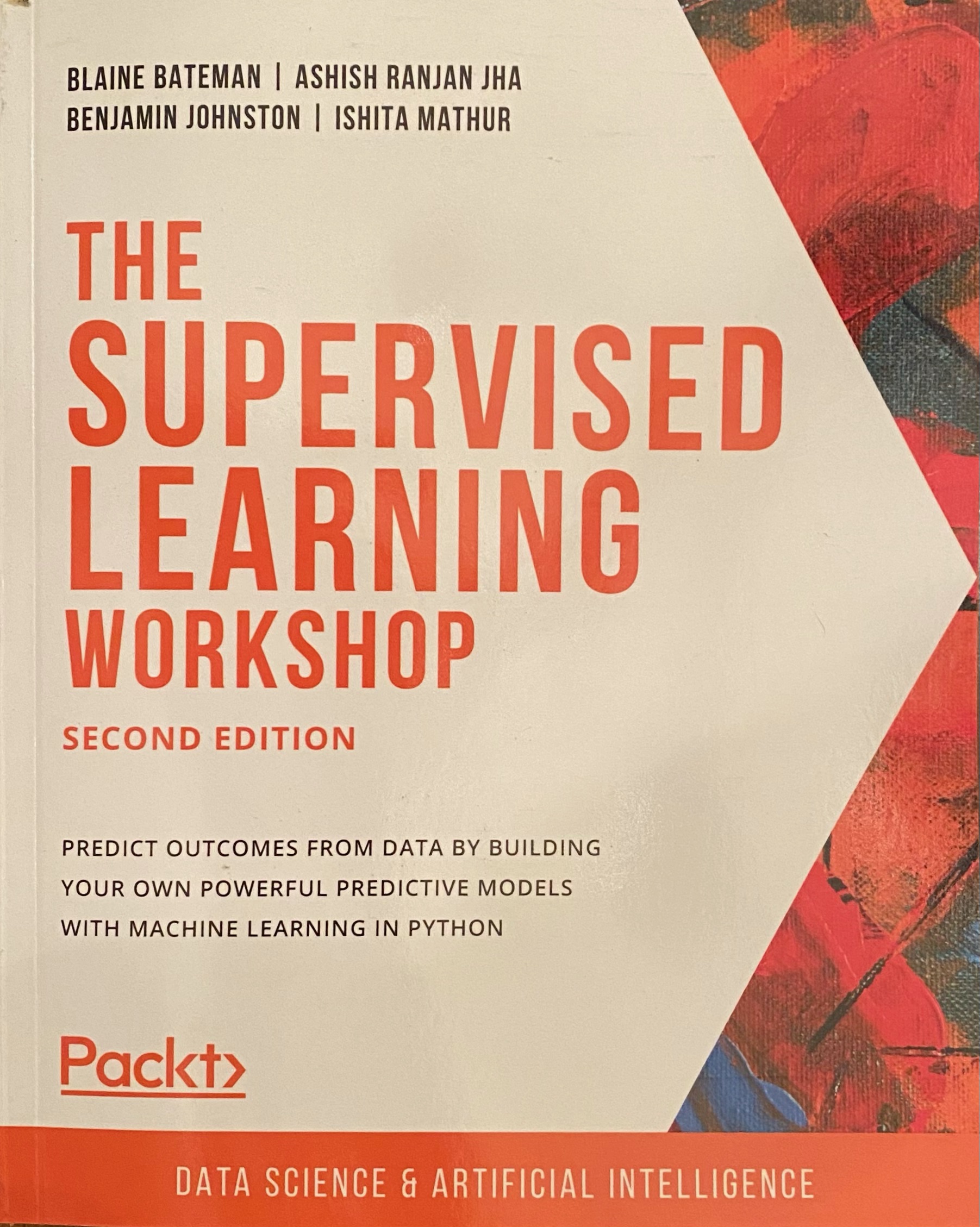
Want to master artificial intelligence (AI) techniques? A new book, The Supervised Learning Workshop, teaches you how to create machine-learning models using the Python programming language. A conversation with the co-author, Blaine Bateman.
Blaine Bateman is a business strategy consultant, helping companies identify growth strategies and opportunities.
Several years ago he decided to focus on data analysis or, more accurately, predictive analytics using machine learning.
“I started to see that clients had lots of data, frequently they didn’t know anything about it and they weren’t using it,” he says. “At the same time, I started to see that AI and machine learning were really on the uptick.”
Machine learning work is also rewarding, he says: “You build stuff and when you get it to work, you do something that helps someone.”
But it is not all fun: there is a lot of “data wrangling”, preparatory work to get the data ready for modelling.
First, the data may need to be integrated if it comes from several sources, and it may need to be scaled. It also pays to study the data, to discover as much as possible about it before modelling. All this takes time.
“Everyone likes the idea that you shovel data into a machine-learning black box and insights come out, but it is not that simple,” says Bateman.
Coming of age
AI and machine learning are terms commonly always mentioned together although machine learning is, in fact, a subset of AI.
There is also no real intelligence here, says Bateman. Machine learning, or what he calls predictive analytics, is the application of tools, algorithms and methodologies to train models.
“That is the learning part and it is using machine – a computer,” he says. “AI sounds a lot cooler but the vast majority of times you see the two, it is one and the same thing.”
AI is also not a new topic: neural networks, genetic algorithms and fuzzy logic were the subjects of much attention in the 1980s and ’90s. But developments in recent years has caused AI to finally hit its stride.
One factor is the maturity of silicon for AI, another is the advent of cloud computing. Bateman also highlights how the AI and machine-learning community embraced the open-source software movement. “It means there is a tremendous amount of commercial-scale work being done using open-source software,” he says.
Google’s TensorFlow, an example of open-source software, is one of the most used libraries for neural networks, while Keras is a software layer that sits on top, simplifying the use of TensorFlow in a Python environment.
“Coding languages such as Python and R have been around a long time and, with the open-source movement, these have grown and been extended into incredibly capable platforms,” says Bateman.
Another important catalyst for AI has been the development of e-learning, or massively open online courses (MOOC).
People used to go to college, learn a skill, enter industry and learn on the job before developing a career. “Now, people are jump-starting that,” he says.
There is an entire industry of people using online courses to learn as fast as possible. “Which is the reason for the books like the one I’ve participated on,” says Bateman.
Supervised learning
Supervised learning refers to data which has a characteristic or property that is known in advance, also referred to as labelled data.
Examples of such data could be numerous images of car registration plates to train an automated road-tolling system, or labelled images of lung abnormalities to train a medical scanning tool.
“We train a model by giving it a picture and telling it the answer,” says Bateman. “Then, once the model is built, you can translate a new picture into an answer.”
There is also unsupervised learning which refers to another aspect of machine learning. Here, data is applied to a clustering algorithm, for example, the MNIST handwritten digits database used to train algorithms to recognise ZIP or postcodes.
The MNIST database can be used for supervised learning, training a model to recognise each of the digits. But in unsupervised learning, the algorithm segregates the digits into clusters without being told what they are.
There are sophisticated clustering methods such as the uniform manifold approximation and projection (UMAP) approach that can reduce complex data sets into smaller dimensions. “It can take up to 80 dimensions and project them onto three and oftentimes find meaningful patterns,” he says.
Yet so far unsupervised learning is not used that much whereas supervised learning accounts for over 80 per cent of all machine learning applications used today, says Bateman.
Book
Packt Publishing wanted to issue a new edition of its machine learning book that included the latest supervised-learning practices. The publisher approached Bateman after seeing his work in the open-source community.
The resulting book – The Supervised Learning Workshop – is aimed at undergraduates and engineers. “Since it jumps into supervised learning, the expectation is that you have some coding skills and know enough Python to work through the exercises,” says Bateman.
The book uses Jupyter Notebooks, an open-source web application for developing Python code. “A lot of people use it to do small projects,” he says.
The topics addressed in the book can all be run using a decent laptop. “A huge amount of people working in AI are working on laptops; it is definitely doable with today’s technology,” he says.
And for larger data sets and bigger problems, there is always the cloud service providers such as Amazon Web Services, Google, Microsoft and others.
After a short introduction covering supervised and unsupervised learning, the book starts with linear regression, which remains an extremely important tool in machine learning.
His advice to students is to build a linear model first and see how well it performs. “That gives you a baseline,” says Bateman.
The topic of gradient-descent is then introduced, a technique used to train more sophisticated algorithms such as neural networks. Further into the book, more sophisticated techniques are introduced.
“The most sophisticated thing we talk about is ways to combine these algorithms into ensembles,” says Bateman.
Ensembling refers to using several less powerful models – what Bateman calls ‘weak learners’ – that are combined in some way, their results may be averaged or their outputs voted on.
Ensembling provides superior results compared with using a single model, even a sophisticated one
Bateman feels lucky to be working in the field of machine learning.
“We have this explosion of freely-available technology that you can use on a laptop to solve amazing problems,” he says. “It is an astonishing time to be a technologist.”

Xilinx’s Versal Premium ready for the 800-gigabit era
When Xilinx was created in 1984, the founders banked on programmable logic becoming ever more attractive due to Moore’s law.
Making logic programmable requires extra transistors so Xilinx needed them to become cheaper and more plentiful, something Moore’s law has delivered, like clockwork, over decades.
Since then, Xilinx’s field-programmable gate array (FPGA) devices have advanced considerably.
Indeed, Xilinx’s latest programmable logic family, the Versal Premium, is no longer referred to as an FPGA but as an adaptive compute accelerator platform (ACAP).
The Versal Premium series of chips, to be implemented using TSMC’s 7nm CMOS process, was unveiled for the OFC 2020 show. The Premium series will have seven chips with the largest, the VP1802, having 50 billion transistors.
First devices will ship in the second half of 2021.
ACAP series
Xilinx unveiled its adaptive compute acceleration platform in 2018.

Kirk Saban
“It is a complete rearchitecting of our device technology,” says Kirk Saban, vice president product and platform marketing at Xilinx. “It is heterogenous by nature and has multiple types of processing engines.”
“Versal Premium is evolutionary compared with previous FPGAs that have hardened blocks for certain functions,” says Bob Wheeler, principal analyst at The Linley Group. “It is another step along a continuum, not really new.”
Six ACAP families are planned for Versal: three tailored for artificial intelligence (AI) - the AI RF, AI Core and AI Edge - and the others being the Prime, Premium and HBM (high bandwidth memory).
Only Versal AI series will have AI engines: very-long-instructing-word (VLIW) processor cores that can also be used for computational-intensive tasks such as digital signal processing.
Premium is the third Versal family to be unveiled, joining the AI Core and Prime series.
Versal Prime is Xilinx’s broadest series in the portfolio, featuring a range of device sizes and capabilities. The Prime series is suited to such applications as storage acceleration in the data centre; wired networking such as 5G back-, mid- and front-haul, and passive optical networking; and industrial applications such as machine vision.
Networking needs
Versal Premium has been developed with core networking and data centre acceleration applications in mind.
“The top-end SKU handles high-end networking applications such as optical transport and data centre interconnect as well as the most demanding signal-processing applications such as radar systems,” says Wheeler.
Xilinx defines core networking as the infrastructure beyond the radio access network. “All the wireline infrastructure is what we consider to be the core of the network,” says Saban. “Access, metro, and core networks, all together.”
When Xilinx’s designers sat down to consider the networking needs for the coming six years, they anticipated a huge capacity hike in the core network. Device numbers are set to grow tenfold with each device generating ten times more traffic.
“The bandwidth going through the wired network globally needs to grow at 50 per cent on a compound annual basis to keep pace with the number of devices being connected and the data coming through them,” says Saban.
Versal Premium will deliver three times the bandwidth and nearly twice the logic capacity of the 16nm Virtex UltraScale+ VU13P FPGA, the largest device used currently for networking and data centre applications.
“Shifts are happening that the Virtex FPGAs are not going to be able to handle,” says Saban. “The move to 400 gigabit and then 800 gigabit on the mid-term horizon, the Virtex products can’t handle that kind of throughput.”
Versal Premium architecture. Source: Xilinx
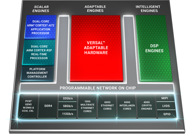
Premium architecture
The Premium devices feature ARM-based scalar processors such as the dual-core Cortex-A72 application processor and the dual-core Cortex-R5F real-time processor.
The application processor is used for general-purpose processing and control. The real-time processor is used for applications that require deterministic processing. Such a processor is key for safety-certified applications.
Also included is a platform management controller that oversees the device. A user can configure many of the ACAP settings using a standard tool flow but the controller’s operation is effectively transparent to the user, says Saban.
The Premium features several types of on-chip memory that Saban likens to levels of cache memory used by high-performance processors. ”We have look-up-table RAM, Block RAM and Ultra RAM and we can offload to [external] DDR4 [RAM],” he says. “The memory hierarchy can be configured to match the algorithm you are building.”
The various on-chip functional blocks are linked via a programmable network-on-a-chip. Having the network-on-a-chip frees up programmable logic resources that would otherwise be required to connect the design’s functional blocks.
“Equipment manufacturers need to deliver on this core network growth but they also need to do it securely,” says Saban. “With everything shifting to the cloud, there are huge concerns about data privacy; in many instances, security is just as important as performance for the operators.”
To this aim, the Premium’s on-chip peripherals include 400-gigabit crypto-engines that support the AES-GCM-256 and -128, MACsec, and IPSec encryption standards.
“The crypto blocks are unique and save a lot of look-up tables and power compared with implementing these in programmable logic,” says Linley’s Wheeler.
Other on-chip features include up to 5 terabits of Ethernet throughput supporting rates from 10 to 400 Gigabit Ethernet. The devices have multiple 600-gigabit Ethernet MAC cores and support such protocols as FlexE, Flex-O, Ethernet CPRI (eCPRI), Fibre Channel over Ethernet (FCoE), and OTN.
The Premium family delivers up to 1.8 terabits of Interlaken, from 10-gigabit to 600-gigabit interfaces. Interlaken enables chip-to-chip and chip-to-backplane communications.
There are also 112-gigabit 4-level pulse-amplitude modulation (PAM-4) serialisers/ deserialisers (serdes). The VP1802 will have 28, 32-gigabit serdes and either 140, 58-gigabit or 70, 112-gigabit serdes. The electrical transceivers can drive 10m of copper cable, says Saban.
PCI Express Generation 5.0, enabling direct memory access and cache-coherent interconnect, is also supported on-chip. “We can connect to server CPUs and be an extension of their memory map,” says Saban.
Xilinx claims 22 UltraScale+ FPGAs would be needed to implement all the logic and peripherals of the Versal Premium VP1802.
System design
Wireline vendors want to double the performance with each generation of equipment while keeping platform size and power consumption constant.
Xilinx has a diagram (shown) of a generic telecom line-card design using the Versal Premium. “Vendors have different variants but at a high-level, they all look like this,” says Saban.
Generic telecom line card using the Versal Premium. Source: Xilinx
Line-card data arrives via optical modules. At present 100-gigabit is mainstream with 400-gigabit coming soon, and eventually 800-gigabit interfaces. The data is fed to the Premium’s hardened logic blocks: the Ethernet and encryption blocks.
The adaptive logic (in red) is what companies use to implement their unique designs such as executing virtualised network functions (NFV) or for packet processing.
“We are seeing the need to infuse artificial intelligence and machine learning into these applications in some capacity,” says Saban. Premium devices have no AI VLIW cores but have sufficient resources for some level of artificial intelligence/ machine learning capability.
Interlaken then sends the data to a host chip or across the backplane to another line card.
Software tools
Xilinx stresses the company is no longer a chip provider but a platform provider. This is reflected in the software tools it provides to accompany its silicon.
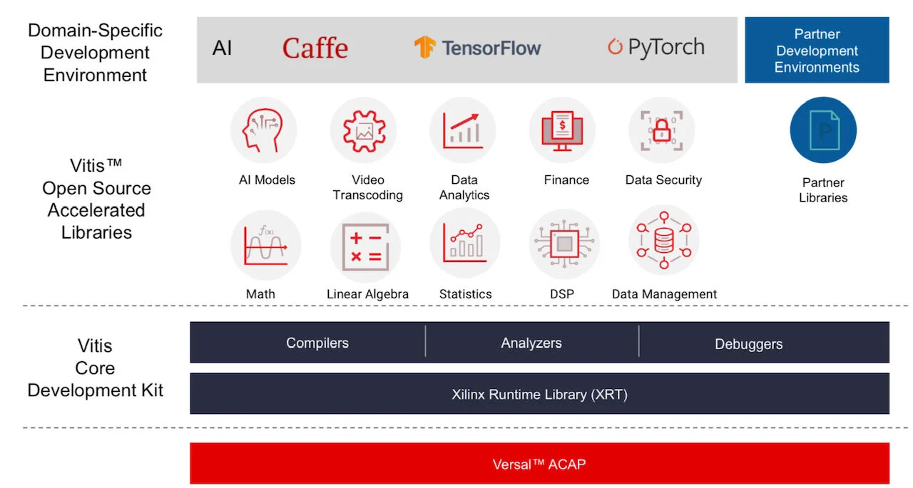
Vitis software tool. Source: Xilinx
Versal ACAPs come with advanced toolkit libraries so engineers can program the chip with no knowledge of the underlying hardware.
Xilinx is continuing to provide its Vivado toolset that supports register-transfer level (RTL), a design abstraction used by hardware engineers for their circuit designs. “The traditional RTL toolchain is not going away and will continue to evolve,” says Saban.
But coders developing data centre applications with no knowledge of RTL or programmable logic can now use Xilinx’s Vitis toolset that was launched in 2019.
“It is critical to enable software developers and data scientists doing machine learning a way to interface to our [ACAP] products,” says Saban.
Vitis supports programming languages such as C, C++ and Python as well as higher-level machine-learning frameworks such as TensorFlow and Caffe.
Xilinx also has a library of functions for tasks such as data analytics and genomics. Such applications can be switched in and out since they are executed using adaptive hardware.
The Premium software tools will be available in the fourth quarter of the year.
Lifespan
A programmable logic family’s lifespan is five or six years; the Virtex UltraScale family was launched in 2015.
“We added a few kickers [to the Virtex family] such as high bandwidth memory and 58-gigabit serdes,” says Saban. “And we will likely do the same with Versal, add some integrated block in a derivative product.”
Xilinx’s chip designers will likely now be already working on an ACAP architecture for 2026 supporting 1.6-terabit speeds and to be implemented using a 5nm CMOS process.
“If we are to deliver twice the bandwidth at half the power, it is not enough to lean on CMOS process technology,” says Saban. “We will need to look at new chip architectures to solve the problems.”
This is challenging. “It gets harder, it gets more expensive and there are less and fewer companies that can afford it,” says Saban.

The key elements of NFV usage: A guide
Orchestration, service assurance, service fulfilment, automation and closed-loop automation. These are important concepts associated with network functions virtualisation (NFV) technology being adopted by telecom operators as they transition their networks to become software-driven and cloud-based.
Prayson Pate (pictured), CTO of the Ensemble division at ADVA Optical Networking, explains the technologies and their role and gives each a status update.
Orchestration
Network functions virtualisation (NFV) is based on the idea of replacing physical appliances - telecom boxes - with software running on servers performing the same networking role.
 Using NFV speeds up service development and deployment while reducing equipment and operational costs.
It also allows operators to work with multiple vendors rather than be dependent on a single vendor providing the platform and associated custom software.
Operators want to adopt software-based virtual network functions (VNFs) running on standard servers, storage and networking, referred to as NFV infrastructure (NFVI).
In such an NFV world, the term orchestration refers to the control and management of virtualised services, composed of virtual network functions and executed on the NFV infrastructure.
The use of virtualised services has created the need for a new orchestration layer that sits between the existing operations support system-billing support system (OSS-BSS) and the NFV infrastructure (see diagram below). This orchestration layer performs the following tasks:
- Manages the catalogue of virtual network functions developed by vendors and by the open-source communities.
- Translates incoming service requests to create the virtualised implementation using the underlying infrastructure.
- Links the virtual network functions as required to create a service, referred to as a service chain. This service chain may be on one server or it may be distributed across the network.
- Performs the various management tasks for the virtual network functions: setting them up, scaling them up and down, updating and upgrading them, and terminating them - the ‘lifecycle management’ of virtual network functions. The orchestrator also ensures their resiliency.
The ETSI standards body, the NFV Industry Specification Group (ETSI NFV ISG), leads the industry effort to define the architecture for NFV, including orchestration.
Several companies are providing proprietary and pre-standard NFV orchestration solutions, including ADVA Optical Networking, Amdocs, Ciena, Ericsson, IBM, Netcracker and others. In addition, there are open source initiatives such as the Linux Foundation Networking Fund’s Open Network Automation Platform (ONAP), ETSI NFV ISG’s Open Source MANO (OSM) and OpenStack’s Tacker initiative.
 Source: ETSI GS NFV 002
Service assurance
Service providers promise that their service will meet a certain level of performance defined in the service level agreement (SLA).
Service assurance refers to the measurement of parameters such as packet loss and latency associated with a service; parameters which are compared against the SLA. Service assurance also remedies any SLA shortfalls. More sophisticated parameters can also be measured such as privacy and responses to distributed denial-of-service (DDOS) attacks.
NFV enables telcos to create and launch services more quickly and economically. But an end customer only cares about the service, not the underlying technology. Customers will not stand for a less reliable service or a service with inferior performance just because it is implemented as a virtual function on a server.
Service assurance is not a new concept, but the nature of a virtualised implementation means a new approach is required. No longer is there a one-to-one association between services and network elements, so the linkages between services, the building-block virtual network functions, and the underlying virtual infrastructure need to be understood. Just as the services are virtualised, so the service assurance process needs virtualised components such as virtual probes and test heads.
The telcos’ operations groups are concerned about how to deploy and support virtualised services. Innovations in service assurance will make their job easier and enable them to do what they could not do before.
EXFO, Ixia, Spirent, and Viavi supply virtual probes and test heads. These may be used for initial service verification, ongoing monitoring, and active troubleshooting. Active troubleshooting is a powerful concept as it enables an operator to diagnose issues without dispatching a technician and equipment.
Service fulfilment
Service fulfilment refers to the configuration and delivery of a service to a customer at one or more locations.
Service fulfilment is essential for an operator because it is how orders are turned into revenue. The more quickly and accurately a service is fulfilled, the sooner the operator gets paid. Prompt fulfilment also leads to greater customer satisfaction and reduced churn.
Early-adopter operators see NFV as a way to improve service fulfilment. Verizon is using its NFV-based service offering to speed up service fulfilment. When a customer orders a service, Verizon instructs the manufacturer to ship a server to the customer. Once connected and powered at the customer’s site, the server calls home and is configured. Combined with optional LTE, a customer can get a service on demand without waiting for a technician. This significantly improves the traditional model where a customer may wait weeks before being able to use the telco’s service.
Network automation
Network automation uses machines instead of trained staff to operate the network. For NFV, the automated software tasks include configuration, operation and monitoring of network elements.
The benefits of network automation include speed and accuracy of service fulfilment - humans can err - along with reduced operational costs.
Telcos have been using network automation for high-volume services and to manage complexity. That said, many operators include manual steps in their process. Such a hands-on approach doesn’t work with cloud technologies such as NFV. Cloud customers can acquire, deploy and operate services without any manual interaction from the webscale players. Likewise, NFV must be automated if telecom operators are to benefit from its potential.
Network automation is closely tied to orchestration. Commercial suppliers and open-source groups are working to ensure that service orders flow automatically from high-level systems down to implementation, dubbed flow-through provisioning and that ‘zero-touch’ provisioning that removes all manual steps becomes a reality. But for this to happen, open and standard interfaces are needed.
Closed-loop automation
Closed-loop automation adds a feedback loop to network automation. The feedback enables the automation to take into account changing network conditions such as loading and network failures, as well as dynamic service demands such as bandwidth changes or services wanted by users.
Closed-loop automation compares the network’s state against rules and policies, replacing what were previously staff decisions. These systems are sometimes referred to as intent-based, as they focus on the desired intent or result rather than on the inputs to the network controls.
Service providers are also investigating adding artificial intelligence and machine learning to closed loop automation. Artificial intelligence and machine learning can replace the hard-coded rules with adaptive and dynamic pattern recognition, allowing anomalies to be detected, adapted to, and even predicted.
Closed-loop automation offloads operational teams not only from manual control but also from manual management processes. Human decisions and planning are replaced by policy-driven control, while human reasoning is replaced by artificial intelligence and machine learning algorithms.
Policy systems or ‘engines’ have existed for a while for functions such as network and file access, but these engines were not closed-loop; there was no feedback. These policy concepts have now been updated to include desired network state, such that a feedback loop is needed to compare the current status with the desired one.
A closed-loop automation system makes dynamic changes to ensure a targeted operational state is reached even when network or service conditions change. This approach enables service providers to match capacity with demand, solve traffic management and network quality issues, and manage 5G and Internet of Things upgrades.
Closed loop automation is complex. Employing artificial intelligence and machine learning will require interfaces to be defined that allow network data into the intelligent systems and enable the outputs to be used.
Several suppliers have announced products supporting closed-loop automation or intent-based networking, including Apstra, Cisco Systems, Forward Networks, Juniper Networks, Nokia, and Veriflow Systems. In addition, the open source ONAP project is also pursuing work in this area.
Xilinx unveils a new class of compute IC
Programmable device company Xilinx has outlined an architecture that it claims represents a new class of computing chip.
The silicon architecture has been four years in the making, involved 1,500 engineers and cost over $1 billion in R&D investment.
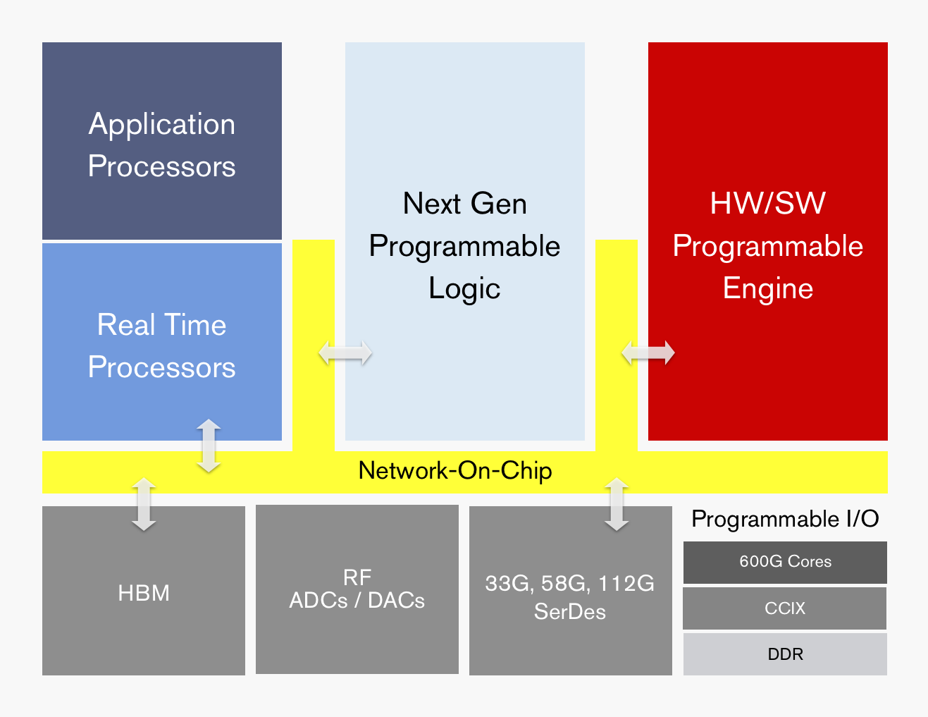 ACAP's functional blocks. Source: Xilinx
Dubbed the adaptive compute acceleration platform (ACAP), the first device will be fabricated using TSMC’s state-of-the-art 7nm CMOS process and will tape out later this year. The largest ACAP devices will use as many as 50 billion transistors.
“Based on the limited information from Xilinx, it is difficult to say what ACAP is, much less whether it creates a new product category,” says Linley Gwennap, principal analyst at The Linley Group.
That said, Gwennap believes the next-generation Xilinx products are far more than simply moving its FPGA technology to a 7nm CMOS. “The company has clearly put significant effort into improving the capabilities of these products to address 5G wireless, machine learning (AI), and other advanced applications,” says Gwennap.
The largest ACAP devices will use as many as 50 billion transistors
Trends
Xilinx says the relentless growth in data coupled with the emergence of artificial intelligence (AI) is driving new computing requirements. At the same time, Moore’s law is slowing down while the speed of innovation is outpacing silicon development cycles.
Victor Peng, Xilinx’s CEO, stresses that while AI is still in its infancy, the technology will be adopted across multiple industries. Thousands of applications will integrate some form of intelligence and this will occur at the network edge and in the cloud. “You will see AI end-to-end,” says Peng.
 Victor Peng
In this new era, chip architectures will be heterogeneous and use processing accelerators. “If you are going to have an intelligent, connected world, it really needs to be adaptable,” says Peng. “It needs to be adaptable because you cannot predict all the needs of the future.”
Gwennap says many companies have already delivered heterogenous chips, given the term heterogeneous refers to a mix of CPU, graphics processor unit (GPU) and digital signal processor (DSP) cores. “This includes every smartphone and PC processor shipping today,” he says.
It also is not clear what ‘adaptive’ means, adds Gwennap: “But if you interpret it to mean FPGA, then both Xilinx and Altera (now Intel) have delivered chips mixing CPUs, DSPs, and FPGAs for years.”
It configures a processor to do a job then, pffft, it has gone
ACAP
Xilinx is not yet detailing the ACAP architecture until the first devices are launched but it has listed the main architectural features.
“Overall, it can be programmed at the hardware level and it has enough architectural features that it can be programmed purely from a software perspective,” says Peng. This means that things can be changed not just at the software level but down at the hardware level, dynamically, while the device is running.
“It configures a processor to do a job then, pffft, it has gone,” says David Manners, the veteran chip journalist at Electronics Weekly who has been covering Xilinx since it was founded in the 1980s.
The ACAP architecture will include both application and real-time processors as well as programmable logic for digital signal processing (DSP) and a hierarchy of distributed memory. The chip will also feature a high-speed network-on-a-chip linking the functional blocks and arbitrating between them.
ACAP will support various generations of DDR memory and certain family devices will include high-bandwidth 3D stacked memory. There will also be device members that use RF analogue-to-digital and digital-to-analogue converters.
In turn, ACAP will have fast input-output circuitry with serial/deserialisers (SERDES) running at 33, 58 and even 112 gigabit-per-second (Gbps) rates. Xilinx demonstrated its latest 112Gbps serdes at the recent OFC show held in San Diego.
Certain ACAP devices will use a novel engine that is software and hardware programmable. Programming the engine at the software level will require some embedded expertise.
“We are always looking at how we can use our hardware programming expertise to get another level of optimisation beyond just software-programmable blocks,” says Peng. Xilinx will detail the engine’s workings later this year.
Xilinx says the 7nm ACAP will deliver a 20x AI compute performance improvement and 4x the 5G communications bandwidth compared to its current 16nm FPGAs.
The company has already delivered software tools for ACAP to select customers and expects first device shipments in 2019.
Data-centre focus
Peng, who has been CEO since January, says the data centre market is now Xilinx’s top priority segment.
Data centres require ever more computing while their networked architectures continue to evolve. This represents an attractive market for Xilinx especially given its programmable devices not only serve computing but also storage and networking requirements.
Xilinx has also been expanding its software development environments that let its devices be programmed at a higher level by developers that have little or no knowledge of the underlying hardware. This contrasts with traditional Xilinx FPGA users that by nature are hardware engineers. “There are easily 1000x more software developers than FPGA developers,” says Peng.
Companies such as Amazon, Alibaba, Huawei, Baidu, Nimbix and Tencent also offer FPGAs-as-a-service as part of their cloud offerings.
The central role of software in data centres may have caused chips to recede into the background, yet Xilinx will argue that the nature of the silicon has never been more important.
Creating a long-term view for the semiconductor industry
The semiconductor industry is set for considerable change over the next 15 years.
“We are at an inflection point in the history of the [chip] industry,” says Thomas Conte, an IEEE Fellow. “It will be very different and very diverse; there won’t be one semiconductor industry.”
Conte (pictured) is co-chair of the IEEE Rebooting Computing initiative that is sponsoring the International Roadmap of Devices and Systems (IRDS) programme (See The emergence of the IRDS, below). The IRDS is defining technology roadmaps over a 15-year horizon and in November will publish its first that spans nine focus areas.
The focus of the IRDS on systems and devices and the broadening of technologies being considered is a consequence of the changing dynamics of the chip industry.
Conte stresses that it is not so much the ending of Moore’s Law that is causing the change as the ending of CMOS. Transistors will still continue to shrink even though it is becoming harder and costlier to achieve but the scaling benefits that for decades delivered a constant power density for chips with each new CMOS process node ended a decade ago.
“Back in the day it was pretty easy to plot it [the roadmap] because the technology was rather static in what we wanted to achieve,” says Conte. That ‘cushy ride’ that CMOS has delivered is ending. “The question now is: Are there other technologies we should be investing in that help applications move forward?” says Conte.
Focus groups
The IRDS has set up nine focus groups and in March published the first white papers from the teams.
The most complete white paper is from the More Moore focus group which looks at how new generations of smaller transistor features will be achieved. “It is clear that for the next 10 to 15 years we still have a lot of CMOS nodes left,” says Conte. “We still have to track what happens to CMOS.”
Conte says it is becoming clearer that ICs, in general, are going to follow the course of flash memory and be constructed as 3D monolithic designs. “We are just beginning to understand how to do this," says Conte.
"This does not mean we are going to get transistors that make computing faster without doing something different,” he says. This explains the work of the Beyond CMOS (Emerging Research Devices) focus team that is looking at alternative non-CMOS technologies to advance systems performance.
It is clear that for the next 10 to 15 years we still have a lot of CMOS nodes left
A third IRDS focus group is Outside System Connectivity which includes interface technologies such as photonic interconnect needed for future systems. “Outside System Interconnect is an important focus group and it is also our interface to the IEEE 5G roadmap team,” he says.
Conte also highlights two other IRDS focus teams: System and Architecture, and Applications Benchmarking. “These two focus teams are really important as to what the IRDS is all about,” says Conte.
The System and Architecture group has identified four systems views that it will focus on: the data centre, mobile handsets and tablets, edge devices for the Internet of Things, and control systems for the cyber-physical world such as automation, robotics and automotive systems.
The Application Benchmarking focus group is tasked with predicting key applications, quantifying how their performance is evolving and identifying roadblocks that could hinder their progress. Feature recognition, an important machine learning task, is one such example.
The IRDS is also continuing the working format established by the ITRS whereby every odd year a new 15-year roadmap is published while updates are published every even year.
Roadmapping
Three communities contribute to the development of the IRDS roadmap: industry, government and academia.
Industry is more concerned with solving their immediate problems and do not have the time or resources to investigate something that might or might not work in 15 years’ time, says Conte. Academia, in contrast, is more interested in addressing challenging problems over a longer term, 15-year horizon. Government national labs in the US and Europe’s imec sit somewhere in between and try to come up with mid-range solutions. “It is an interesting tension and it seems to work,” says Conte.
Contributors to the IRDS are from the US, Europe, Japan, South Korea and Taiwan but not China which is putting huge effort to be self-sufficient in semiconductors.
“We have not got participation for China yet,” says Conte. “It is not that we are against that, we just have not made the connections yet.” Conte believes China’s input would be very good for the roadmap effort. “They are being very aggressive and bright and they are more willing to take risks than the West,” he says.
What will be deemed a success for the IRDS work?
“It is to come up with a good prediction that is 15 years out and identify what the roadblocks are to getting there.”
____________________________________________________________
The emergence of the IRDS
The IRDS was established in 2016 by the IEEE after it took over the roadmap work of the International Technology Roadmap for Semiconductors (ITRS), an organisation sponsored by the five leading chip manufacturing regions in the world.
“The [work of the] ITRS was a bottoms-up roadmap, driven by the semiconductor industry,” says Conte. “It started with devices and didn't really go much higher.”
With the end of scaling, whereby the power density of chips remained constant with each new CMOS process node, the ITRS realised its long-established roadmap work needed a rethink which resulted in the establishment of ITRS 2.0.
“The ITRS 2.0 was an attempt to do a top-down approach looking at the system level and working down to devices,” says Conte. It was well received by everyone but the sponsors, says Conte, which was not surprising given their bottoms-up focus. It resulted in the sponsors of the ITRS 2.0 such as the US Semiconductor Industry Association (SIA) pulling out and the IEEE stepping in.
“This is much closer to what we are trying to do with the Rebooting Computing so it makes sense this group comes into the IEEE band and we act as a sponsor,” says Conte.