
Stitching together disaggregated chips
The Optical Internetworking Forum (OIF) has begun work on a 112-gigabit electrical interface to connect chips in a multi-chip module.
The ultra-short-reach electrical interface for multi-chip modules adds to the OIF's ongoing CEI-112G project, started in August 2016, to develop a 112 gigabit-per-second (Gbps) serial electrical interface for next-generation optical modules.
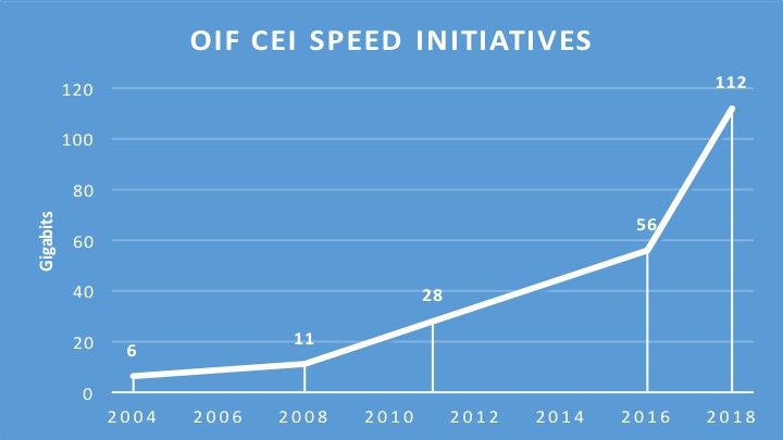 Source: Gazettabyte, OIF data. The year 2018 is an estimate.
The OIF is an industry organisation whose members include telcos, data centre operators, equipment makers and component companies. The OIF undertakes projects that range from high-speed interfaces, optical modules and flexible Ethernet through to programmable interfaces for Transport SDN. Each OIF project culminates in a published Implementation Agreement.
According to David Stauffer, of Kandou Bus and the OIF’s Physical and Link Layer Working Group Chair, the 112G multi-chip module initiative builds on earlier OIF work on a 56-gigabit ultra-short-reach (USR) interface that first addressed die-to-die communication. "We realised that there seems to be more than one application," says Stauffer. "The 112G project is expanded for these applications such that we will possibly end up with different solutions rather than just one."
Multi-chip modules
It was during the 56G USR work that the OIF first heard from members about the challenges of designing a system-on-chip and the idea of taking functions off-chip. High-capacity Ethernet switch chips, for example, are becoming so complex that future designs will not be able to support the long-reach serialisers-deserialisers (SerDes) circuits used for input-output due to the resulting design exceeding the chip's power constraints. “They [chip makers] were starting to think about offloading functions such as SerDes from the system-on-chip,” says Stauffer.
State-of-the-art chip designs can also include functions that occupying significant die area. “To better optimise chip and system costs, people are starting to think about the concept of breaking up the system-on-chip into multiple chips that are better optimised for cost and yield,” says Stauffer. He cites as an example a next-generation system-on-chip that interfaces to long-reach SerDes or optics, performs sensor processing and has significant on-board logic.
 David StaufferThe logic functions of such a chip are best implemented using an advanced 7nm CMOS process, yet SerDes design are not implemented in 7nm and won't be for some time yet. In turn, the sensor array may not even be implemented using a logic process. And if the logic circuitry occupies a significant die area, it may be more economical to split the logic into two chips, each of which will yield better. “Then I have a need for all these interfaces between these chips,” says Stauffer,
He stresses that the interfaces are split based on the the type of technology and on the size of the individual dies; the dies are not partitioned to minimise the bandwidth between them. This can result in significant bandwidth - terabits of capacity - between chips in the module. And to be cost-effective, the interfaces must be very low power.
Accordingly, interfaces between two logic chips or the logic function and the sensor array can require high bandwidth whereas interfaces to the SerDes may be a single lane and have different requirements in how it is clocked. “So there is some divergence in what may be the requirements,” says Stauffer. “The multi-chip module project allows for the fact that we may end up with two solutions.”
The OIF does not list companies involved in its projects. Kandou Bus is clearly one involved in the multi-chip module work, says Stauffer, and he points to similar work his company has done with Marvell but at lower rates. But a recent story in EETimes lists several companies.
Applications
Stauffer says there are several high-performance computing companies that are designing very high-end processing systems using new architectures. “They are going to use this stuff [multi-chip modules and 100G-plus interfaces] before it trickles down to the data centre,” he says.
For applications requiring sensor arrays, the sampling and control loops needed mean that in some cases the interface will need to support terabits-per-second of capacity, says Stauffer; the overall interface speed depending on the number of sensors in the array and the rate at which they sample.
The OIF ultra-short-reach interface is expected to work up to 116Gbps. Some members also want the interface to drive optical devices. “There is going to be a single lane interface at 100G-plus and others that consist of many parallel lanes,” says Stauffer.
The interface will operate over distances of 1cm to 2cm depending on the interposer technology used in the multi-chip module. Using an organic interposer will enable a reach of up to 2cm whereas a silicon interposer the distances will be 1cm or less.
A silicon interposer can be seen as a chip designed solely to interconnect the chips that sit on top, says Stauffer. The advantage of a silicon interposer is that it can supports thousands of input-outputs. But depending on its size and yield, the silicon interposer can be expensive. It also has higher-loss channels, explaining its shorter 1cm reach.
In contrast, an organic interposer is more in line with traditional multi-chip modules, says Stauffer. The interconnect density of an organic interposer is less than a silicon one due to the relatively large pad pitches it uses but the organic interposer is cheaper and has a lower insertion loss. “The OIF is designing something that is suitable for both,” says Stauffer.
No timetable has been given as to the duration of the multi-chip module interface work. But Stauffer says there are companies that would use the electrical interface now if it were available.
Altera’s 30 billion transistor FPGA
- The Stratix 10 features a routing architecture that doubles overall clock speed and core performance
- The programmable family supports the co-packaging of transceiver chips to enable custom FPGAs
- The Stratix 10 family supports up to 5.5 million logic elements
- Enhanced security features stop designs from being copied or tampered with
Altera has detailed its most powerful FPGA family to date. Two variants of the Stratix 10 family have been announced: 10 FPGAs and 10 system-on-chip (SoC) devices that include a quad-core 64-bit architecture Cortex-A53 ARM processor alongside the programmable logic. The ARM processor can be clocked at up to 1.5 GHz.
The Stratix 10 family is implemented using Intel’s 14nm FinFET process and supports up to 5.5 million logic elements. The largest device in Altera’s 20nm Arria family of FPGAs has 1.15 million logic elements, equating to 6.4 billion transistors. “Extrapolating, this gives a figure of some 30 billion transistors for the Stratix 10,” says Craig Davis, senior product marketing manager at Altera.
 Altera's HyperFlex routing architecture. Shown (pointed to by the blue arrow) are the HyperFlex registers that sit at the junction of the interconnect traces. Also shown are the adaptive logic module blocks. Source: Altera.
The FPGA family uses a routing fabric, dubbed HyperFlex, to connect the logic blocks. HyperFlex is claimed to double the clock speed compared to designs implemented using Altera’s Stratix V devices, to achieve gigahertz rates. “Having that high level of performance allows us to get to 400 gigabit and one terabit OTN (Optical Transport Network) systems,” says Davies.
The FPGA company detailed the Stratix 10 a week after Intel announced its intention to acquire Altera for US $16.7 billion.
Altera is also introducing with the FPGA family what it refers to as heterogeneous 3D system packaging and integration. The technology enables a designer to customise the FPGA’s transceivers by co-packaging separate transceiver integrated circuits (ICs) alongside the FPGA.
Different line-rate transceivers can be supported to meet a design's requirements: 10, 28 or 56 gigabit-per-second (Gbps), for example. It also allows different protocols such as PCI Express (PCIe), and different modulation formats including optical interfaces. Altera has already demonstrated a prototype FPGA co-packaged with optical interfaces, while Intel is developing silicon photonics technology.
HyperFlex routing
The maximum speed an FPGA design can be clocked is determined by the speed of its logic and the time it takes to move data from one part of the chip to another. Increasingly, it is the routing fabric rather than the logic itself that dictates the total delay, says Davis.
This has led the designers of the Stratix 10 to develop the HyperFlex architecture that adds a register at each junction of the lines interconnecting the logic elements.
Altera first tackled routing delay a decade ago by redesigning the FPGA’s logic building block. Altera went from a 4-input look-up table logic building block to a more powerful 8-input one that includes output registers. Using the more complex logic element - the adaptive logic module (ALM) - simplifies the overall routing. “You are essentially removing one layer of routing from your system,” says Davies.
When an FPGA is programmed, the file is presented that dictates how the wires and hence the device’s logic are connected. The refinement with HyperFlex is that there are now registers at those locations where the switching between the traces occurs. A register can either be bypassed or used.
“It allows us to put the registers anywhere in the design, essentially placing them in an optimum place for a given route across the FPGA,” says Davies. The number of hyper-registers in the device's routing outnumber the standard registers in the ALM blocks by a factor of ten.
Using the registers, designers can introduce data pipelining to reduce overall delay and it is this pipelining, combined with the advanced 14nm CMOS process, that allows a design to run at gigahertz rates.
“We have made the registers small but they add one or two percent to the total die area, but in return it gives us the ability to go to twice the performance,” says Davies. “That is a good trade-off.
The biggest change getting HyperFlex to work has been with the software tools, says Davies. HyperFlex and the associated tools has taken over three years to develop.
“This is a fundamental change,” says Davies. “It [HyperFlex] is relatively simple but it is key; and it is this that allows customers to get to this doubling of core performance.”
The examples cited by Altera certainly suggest significant improvements in speed, density, power dissipation, but I want to see that in real-world designs
Loring Wirbel, The Linley Group
Applications
Altera says that over 100 customer designs have now been processed using the Stratix 10 development tools.
It cites as an example a current 400 gigabit design implemented using a Stratix V FPGA that requires a bus 1024-bits wide, clocked at 390MHz. The wide bus consumes considerable chip area and routing it to avoid congestion is non-trivial.
Porting the design to a Stratix 10 enables the bus to be clocked at 781MHz such that the bus width can be halved to 512 bits. “It reduces congestion, makes it easier to do timing closure and ship the design,” says Davies. “This is why we think Stratix 10 is so important for high-performance applications like OTN and data centres.” Timing closure refers to the tricky part of a design where the engineer may have to iterate to ensure that a design meets all the timing requirements.
For another, data centre design, a Stratix 10 device can replace five Stratix V ICs on one card. The five FPGAs are clocked at 250MHz, run PCIe Gen2 x8 interfaces and DDR3 x72 memory clocked at 800MHz. Overall the power consumed is 120W. Using one Stratix 10 chip clocked at 500MHz, faster PCIe Gen3 x8 can be supported as can a wider DDR3 x144 memory clocked at 1.2GHz, with only 44W consumed.
Loring Wirbel, senior analyst at The Linley Group, says that Altera’s insertion of pipelined registers to cut average trace lengths is unique.
“The more important question is, can the hyper-register topology regularly gain the type of advantages claimed?” says Wirbel. “The examples cited by Altera certainly suggest significant improvements in speed, density, power dissipation, but I want to see that in real-world designs.”
We are also looking at optical transceivers directly connected to the FPGA
Craig Davies, Altera
Connectivity tiles
Altera recognises that future FPGAs will support a variety of transceiver types. Not only are there different line speeds to be supported but also different modulation schemes. “You can’t build one transceiver that fits all of these requirements and even if you could, it would not be an optimised design,” says Davies.
Instead, Altera is exploiting Intel’s embedded multi-die interconnect bridge (EMIB) technology to interface the FPGA and transceivers, dubbed connectivity tiles. The bridge technology is embedded into the chip’s substrate and enables dense interconnect between the core FPGA and the transceiver IC.
Intel claims fewer wafer processing steps are required to make the EMIB compared to other 2.5D interposer processes. An interposer is an electrical design that provides connectivity. “This is a very simple ball-grid sort of interposer, nothing like the Xilinx interposer,” says Wirbel. “But it is lower cost and not intended for the wide range of applications that more advanced interposers use.”
Using this approach, a customer can add to their design the desired interface, including optical interfaces as well as electrical ones. “We are also looking at optical transceivers directly connected to the FPGA,” says Davies.
Wirbel says such links would simplify interfacing to OTN mappers, and data centre designs that use optical links between racks and for the top-of-rack switch.
“Intel wants to see a lot more use of optics directly on the server CPU board, something that the COBO Alliance agrees with in part, and they may steer the on-chip TOSA/ ROSA (transmitter and receiver optical sub-assembly) toward intra-board applications,” he says.
But this is more into the future. “It's fine if Intel wants to pursue those things, but it should not neglect common MSAs for OTN and Ethernet applications of a more traditional sort,” says Wirbel.
The benefit of the system-in-package integration is that different FPGAs can be built without having to create a new expensive mask set each time. “You can build a modular lego-block FPGA and all that it has different is the packaged substrate,” says Davies.
Security and software
Stratix 10 also features security features to protect companies’ intellectual property from being copied or manipulated.
The FPGA features security hardware that protects circuitry from being tampered with; the bitstream that is loaded to configure the FPGA must be decrypted first.
The FPGA is also split into sectors such that parts of the device can have different degrees of security. The sectoring is useful for cloud-computing applications where the FPGA is used as an accelerator to the server host processor. As a result, different customers’ applications can be run in separate sectors of the FPGA to ensure that they are protected from each other.
The security hardware also allows features to be included in a design that the customer can unlock and pay for once needed. For example, a telecom platform could be upgraded to 100 Gigabit while the existing 40 Gig live network traffic runs unaffected in a separate sector.
Altera has upgraded its FPGA software tools in anticipation of the Stratix 10. Features include a hierarchical design flow to simplify the partitioning of a design project across a team of engineers, and the ability to use cloud computing to speed up design compilation time.
What applications will require such advanced FPGAs, and which customers will be willing to pay a premium price for? Wirbel says the top applications will remain communications.
“The emergence of new 400 Gig OTN transport platforms, and the emergence of all kinds of new routers and switches with 400 Gig interfaces, will keep a 40 percent communication base for FPGAs overall solid at Altera,” he says.
Wirbel also expects server accelerator boards where FPGA-based accelerators are used for such applications as financial trading and physics simulation will also be an important market. “But Intel must consider the accelerator board market as an ideal place for Stratix 10 on its own, and not merely as a vehicle for promoting a future Xeon-plus-FPGA hybrid,” he says.
Altera will have engineering samples of the Stratix 10 towards the end of 2015, before being shipped to customers.