
Packaging silicon photonics using passive alignment
- An Israeli start-up is tackling a key packaging challenge for silicon photonics
Teramount has developed a way to simplify the packaging of silicon photonics chips. Instead of using active alignment whereby an external laser is required to carefully align a fibre to the optical die, the Israeli start-up has developed a technology that allows passive alignment.
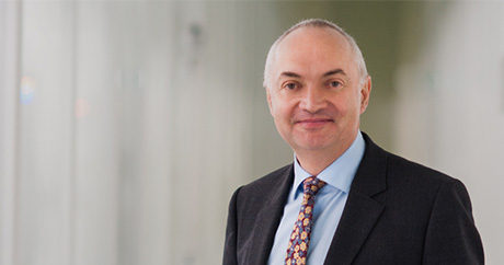
 Hesham Taha“If we want silicon photonics to ramp up to volume, it has to meet CMOS standards both in terms of fabrication and packaging,” says Hesham Taha, Teramount's CEO.
Taha worked at a company developing atomic force microscopy systems before co-founding Teramount. "We got to know of the problem of injecting light into a waveguide and were surprised that the industry was still using active alignment," he says.
This spurred Taha and a colleague to develop optical solutions to match a single-mode fibre core to an optical waveguide, and they founded Teramount in Jerusalem in 2013. "We started real activity at the beginning of 2015 after getting funding," says Taha.
Existing silicon photonics companies either develop their own customised active alignment equipment or outsource the activity to a third party. "If we solve one of the bottlenecks of silicon photonics in terms of packaging, silicon photonics will be more and more adopted," says Taha.
If we want silicon photonics to ramp up to volume, it has to meet CMOS standards both in terms of fabrication and packaging
The design
Teramount's solution includes two elements: a PhotonicsPlug that is flip-chipped onto the silicon photonics die while still part of a wafer, and a 'bump', a design element added on the silicon photonics chip next to the optical waveguide. "Our solution, which we will be selling, is the PhotonicsPlug and we do require them [the designers] to add one element [the bump] to their silicon photonics chip," says Taha.
The main PhotonicsPlug component is a silicon die comprising optics that manipulates the beam using self-aligning optics and focusses it onto the silicon photonics chip via a glass spacer. Teramount’s die also has V-grooves to interface the single-mode ribbon fibre. Teramount says its die is made using an inexpensive mature CMOS process due to the relatively large feature sizes of the optical elements.
The second design element - the bump - is added next to the silicon photonics chip's grating coupler. The grating coupler is one of two techniques used in the industry to interface a fibre to the waveguide, the other being edge coupling.
“We want to place it [the bump] next to the waveguide so that the optics of the PhotonicPlug works in conjunction with it so that it brings the beam to the waveguide with a large tolerance,” says Taha. The bump is accurately placed on the chip using standard lithography techniques.
The resulting tolerance with which the die can be attached to the silicon photonics wafer is up to ± 20 microns in each of the three dimensions such that standard flip-chip machines can attach the PhotonicsPlug to the wafer.
“Flip-chip machines today work with a tolerance of ± 6 microns and can do 1,500 assemblies per hour,” says Taha.
"This is the main philosophy we are bringing here," he says. "Instead of the accurate placement of the fibre next to the grating coupler which requires active alignment, we want to replace that with a cheaper alignment technique that has much better accuracy at the wafer level," says Taha.
Status
Teramount has already shown working devices using the technology. In addition, Teramount is working with several partners and has demonstrated its technology with their silicon photonics chip designs. "With these partners we are doing the integration and qualifying the performance of the device," says Taha. "We will finalise at least two of these partnerships within a few months."
The start-up is also working to enable volume manufacturing by bringing its technology to industrial fabrication plants. This will be completed in the next few months.
Being a small start-up, the company is focussed on developing the grating coupler solution but it has already started work on an edge-coupling technique to a device’s waveguides. Edge coupling is suited to wavelength-division multiplexing (WDM) silicon photonics chips. That is because grating couplers are wavelength-dependent while edge coupling supports a broader range of wavelengths.
IoT will drive chip design and new styles of computing
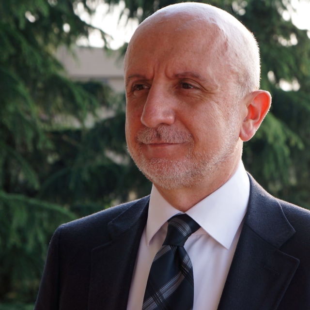
Looking back 20 years hence, how will this period be viewed? The question was posed by the CEO of imec, Luc Van de hove, during his opening talk at a day event imec organised in Tel-Aviv.
For Van den hove, this period will be seen as one of turbulent technological change. “The world is changing at an incredible rate,” he says. “The era of digital disruption is changing our industry and this disruption is not going to stop.”
 Luc Van den hove
It was the Belgium nonoelectronics R&D centre’s second visit to Israel to promote its chip and systems expertise as it seeks to expand its links with Israel’s high-tech industry. And what most excites imec is the Internet of Things (IoT), the advent of connected smart devices that turn data into information and adapt the environment to our needs.
The world is changing at an incredible rate. The era of digital disruption is changing our industry and this disruption is not going to stop
Internet of Things
Imec is focussing on five IoT areas: Smart Health - wearable and diagnostic devices, Smart Mobility which includes technologies for autonomous cars, drones and robots, Smart Cities, Smart Industry and Smart Energy. “In all these areas we look at how we can leverage our semiconductor know-how,” says Van den hove. “How we can bring innovative solutions by using our microchip technology.”
The broad nature of the IoT means imec must form partnerships across industries while strengthening its systems expertise. In healthcare, for example, imec is working with John Hopkins University, while last October, imec completed the acquisition of iMinds, a Belgium research centre specialising in systems software and security.
“One of the challenges of IoT is that there is not one big killer application,” says Van den hove. “How to bring these technologies to market is a challenge.” And this is where start-ups can play a role and explains why imec is visiting Israel, to build its partnerships with local high-tech firms.
Imec also wants to bring its own technologies to market through start-ups and has established a €100 million investment fund to incubate new ideas and spin-offs.
Technologies
Imec’s expertise ranges from fundamental semiconductor research to complex systems-on-chip. It is focussing on advanced sensor designs for IoT as this is where it feels it can bring an advantage. Imec detailed a radar chip design for cars that operates at 79GHz yet is implemented in CMOS. It is also developing a Light Detection and Ranging (LIDAR) chip for cars based on integrated photonics. Future cars will have between 50 to 100 sensors including cameras, LIDAR, radar and ultrasound.
 Imec's multi-project wafers. Source: imec
The data generated from these sensors must be processed, fused and acted upon. Imec is doing work in the areas of artificial intelligence and machine learning. In particular, it is developing neuromorphic computing devices that use analogue circuits to mimic the biological circuitry of the brain. Quantum computing is another area imec has begun to explore.
One of the challenges of IoT is that there is not one big killer application
“There is going to be so much data generated,” says Van den Hove. “And it is better to do it [processing] locally because computation is cheaper than bandwidth.”
Imec envisages a network with layers of intelligence, from the sensors all the way to the cloud core. As much of the data as possible will be processed by the sensor so that it can pass on more intelligent information to the network edge, also known as fog computing. Meanwhile, the cloud will be used for long-term data storage, for historical trending and for prediction using neuromorphic algorithms, says Van den Hove.
But to perform intensive processing on-chip and send the results off-chip in a power-efficient manner will require advances in semiconductor technology and the continuation of Moore’s law.
Moore's law
Imec remains confident that Moore’s law will continue to advance for some years yet but notes it is getting harder. In the past, semiconductor technology had a predictable roadmap such that chip designers could plan ahead and know their design goals would be met. Now chip technologists and designers must work together, a process dubbed technology-design co-optimisation.
Van den hove cites the example of imec’s work with ARM Holdings to develop a 7nm CMOS process node. “You can create some circuit density improvement just by optimising the design, but you need some specific technology features to do that,” he says. For example, by using a self-alignment technique, fewer metal tracks can be used when designing a chip's standard cell circuitry. "Using the same pitch you get an enormous shrink," he says. But even that is not going to be enough and techniques such as system-technology co-optimisation will be needed.
Imec is working on FinFETs, a style of transistor, to extend CMOS processes down to 5nm and then sees the use of silicon nanowire technology - first horizontal and then vertical designs - to extend the roadmap to 3nm, 2.5nm and even 1.8nm feature sizes.
Imec is also working on 3D chip stacking techniques that will enable multi-layer circuits to be built. “You can use specific technologies for the SRAM, processing cores and the input-output.” Imec is an active silicon photonics player, seeing the technology playing an important role for optical interconnect.
Imec awarded Gordon Moore a lifetime of innovation award last year, and Van den hove spent an afternoon at Moore’s home in Hawaii. Van den hove was struck with Moore’s humility and sharpness: “He was still so interested in the technology and how things were going.”
Silicon photonics adds off-chip comms to a RISC-V processor
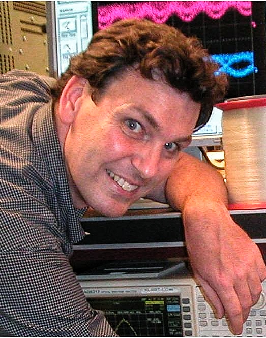
"For the first time a system - a microprocessor - has been able to communicate with the external world using something other than electronics," says Vladimir Stojanovic, associate professor of electrical engineering and computer science at the University of California, Berkeley.
 Vladimir Stojanovic
The microprocessor is the result of work that started at MIT nearly a decade ago as part of a project sponsored by the US Defense Advanced Research Projects Agency (DARPA) to investigate the integration of photonics and electronics for off-chip and even intra-chip communications.
The chip features a dual-core 1.65GHz RISC-V open instruction set processor and 1 megabyte of static RAM and integrates 70 million transistors and 850 optical components.
The work is also notable in that the optical components were developed without making any changes to an IBM 45nm CMOS process used to fabricate the processor. The researchers have demonstrated two of the processors communicating optically, with the RISC core on one chip reading and writing to the memory of the second device and executing programs such as image rendering.
This CMOS process approach to silicon photonics, dubbed 'zero-change' by the researchers, differs from that of the optical industry. So far silicon photonics players have customised CMOS processes to improve the optical components' performance. Many companies also develop the silicon photonics separately, using a trailing-edge 130nm or 90nm CMOS process while implementing the driver electronics on a separate chip using more advanced CMOS. That is because photonic devices such as a Mach-Zehnder modulator are relatively large and waste expensive silicon real-estate if implemented using a leading-edge process.
IBM is one player that has developed the electronics and optics on one chip using a 90nm CMOS process. However, the company says that the electronics use feature sizes closer to 65nm to achieve electrical speeds of 25 gigabit-per-second (Gbps), and being a custom process, it will only be possible to implement 50-gigabit rates using 4-level pulse amplitude modulation (PAM-4).
We are now reaping the benefits of this very precise process which others cannot do because they are operating at larger process nodes
"Our approach is that photonics is sort of like a second-class citizen to transistors but it is still good enough," says Stojanovic. This way, photonics can be part of an advanced CMOS process.
Pursuing a zero-change process was first met with skepticism and involved significant work by the researchers to develop. "People thought that making no changes to the process would be super-restrictive and lead to very poor [optical] device performance," says Stojanovic. Indeed, the first designs produced didn't work. "We didn't understand the IBM process and the masks enough, or it [the etching] would strip off certain stuff we'd put on to block certain steps."
But the team slowly mastered the process, making simple optical devices before moving on to more complex designs. Now the team believes its building-block components such as its vertical grating couplers have leading-edge performance while its ring-resonator modulator is close to matching the optical performance of designs using custom CMOS processes.
"We are now reaping the benefits of this very precise process which others cannot do because they are operating at larger process nodes," says Stojanovic.
Silicon photonics design
The researchers use a micro ring-resonator for its modulator design. The ring-resonator is much smaller than a Mach-Zehnder design and is 10 microns in diameter. Stojanovic says the dimensions of its vertical grating couplers are 10 to 20 microns while its silicon waveguides are 0.5 microns.
Photonic components are big relative to transistors, but for the links, it is the transistors that occupy more area than the photonics. "You can pack a lot of utilisation in a very small chip area," he says.
A key challenge with a micro ring-resonator is ensuring its stability. As the name implies, modulation of light occurs when the device is in resonance but this drifts with temperature, greatly impairing its performance.
Stojanovic cites how even the bit sequence can affect the modulator's temperature. "Given the microprocessor data is uncoded, you can have random bursts of zeros," he says. "When it [the modulator] drops the light, it self-heats: if it is modulating a [binary] zero it gets heated more than letting a one go through."
The researchers have had to develop circuitry that senses the bit-sequence pattern and counteracts the ring's self-heating. But the example also illustrates the advantage of combining photonics and electronics. "If you have a lot of transistors next to the modulator, it is much easier to tune it and make it work," says Stojanovic.
 A prototype set-up of the chip-to-chip interconnect using silicon photonics. Source: Vladimir Stojanovic
Demonstration
The team used two microprocessors - one CPU talking to the memory of the second chip 4m away. Two chips were used rather than one - going off-chip before returning - to prove that the communication was indeed optical since there is also an internal electrical bus on-chip linking the CPU and memory. "We wanted to demonstrate chip-to-chip because that is where we think the biggest bang for the buck is," says Stojanovic.
In the demonstration, a single laser operating at 1,183nm feeds the two paths linking the memory and processor. Each link is 2.5Gbps for a total bandwidth of 5Gbps. However the microprocessor was clocked at one-eightieth of its 1.65GHz clock speed because only one wavelength was used to carry data. The microprocessor design can support 11 wavelengths for a total bandwidth of 55Gbit/s while the silicon photonics technology itself will support between 16 and 32 wavelengths overall.
The group is already lab-testing a new iteration of the chip that promises to run the processor at full speed. The latest chip also features improved optical functions. "It has better devices all over the place: better modulators, photo-detectors and gratings; it keeps evolving," says Stojanovic.
We can ship that kind of bandwidth [3.2 terabits] from a single chip
Ayar Labs
Ayar Labs is a start-up still in stealth mode that has been established to use the zero-change silicon photonics to make interconnect chips for platforms in the data centre.
Stojanovic says the microprocessor demonstrator is an example of a product that is two generations beyond existing pluggable modules. Ayar Labs will focus on on-board optics, what he describes as the next generation of product. On-board optics sit on a card, close to the chip. Optics integrated within the chip will eventually be needed, he says, but only once applications require greater bandwidth and denser interfaces.
"One of the nice things is that this technology is malleable; it can be put in various form factors to satisfy different connectivity applications," says Stojanovic.
What Ayar Labs aims to do is replace the QSFP pluggable modules on the face plate of a switch with one chip next to the switch silicon that can have a capacity of 3.2 terabits. "We can ship that kind of bandwidth from a single chip," says Stojanovic.
Such a chip promises cost reduction given how a large part of the cost in optical design is in the packaging. Here, packaging 32, 100 Gigabit Ethernet QSFP modules can be replaced with a single optical module using the chip. "That cost reduction is the key to enabling deeper penetration of photonics, and has been a barrier for silicon photonics [volumes] to ramp," says Stojanovic.
There is also the issue of how to couple the laser to the silicon photonics chip. Stojanovic says such high-bandwidth interface ICs require multiple lasers: "You definitely don't want hundreds of lasers flip-chipped on top [of the optical chip], you have to have a different approach".
Ayar Labs has not detailed what it is doing but Stojanovic says that its approach is more radical than simply sharing one laser across a few links, "Think about the laser as the power supply to the box, or maybe a few racks," he says.
The start-up is also exploring using standard polycrystalline silicon rather than the more specialist silicon-on-isolator wafers.
"Poly-silicon is much more lossy, so we have had to do special tricks in that process to make it less so," says Stojanovic. The result is that changes are needed to be made to the process; this will not be a zero-change process. But Stojanovic says the changes are few in number and relatively simple, and that it has already been shown to work.
Having such a process available would allow photonics to be added to transistors made using the most advanced CMOS processes - 16nm and even 7nm. "Then silicon-on-insulator becomes redundant; that is our end goal,” says Stojanovic.
Further information
Single-chip microprocessor that communicates directly using light, Nature, Volume 528, 24-31 December 2015
Moore's law and silicon photonics
Chip pioneer Gordon E. Moore’s article appeared in the magazine Electronics in 1965. Dr. Moore was the director of the R&D labs at Fairchild Semiconductor, an early maker of transistors. Moore went on to co-found Intel, then a memory company, becoming its second CEO after Robert Noyce.
Moore’s article was written in the early days of integrated circuits. At the time, silicon wafers were one inch in diameter and integrating 50 components on a chip was deemed a state-of-the-art design.
Moore observed that, at any given time, there was an ideal number of components that achieved a minimum cost. Add a few more components and the balance would be tipped: the design would become overly complex, wafer yields would go down and costs would rise.
His key insight, later to become known as Moore’s law, was that integrated circuit complexity at this minimum cost was growing over time. Moore expected the complexity to double each year for at least another decade.
In his article he predicted that, by 1970, the manufacturing cost per component would be a tenth of the cost in 1965. Extrapolating the trend further, Moore believed that “by 1975, the number of components per integrated circuit for minimum cost will be 65,000 components.” Moore was overly optimistic, but only just: in 1975, Intel was developing a chip with 32,000 transistors.
“Perhaps we can say that the future of silicon photonics is the future of electronics itself.”
One decade after his article, Moore amended his law to a doubling of complexity every 24 months. By then the industry had started talking about transistors rather than components - circuit elements such as transistors, resistors and capacitors - after alighting on complementary metal oxide semiconductor (CMOS) technology to make the bulk of its chips. And in the years that followed, the period of complexity-doubling settled at every 18 months.
Moore has received less credit for his article's remarkable foresight regarding the importance of integrated circuits, especially when, in 1965, their merits were far from obvious. Such devices would bring a proliferation of electronics, he said, “pushing this science into many new areas”.
He foresaw home computers “or at least terminals connected to a central computer’, automatic control for automobiles and even mobile phones - ‘personal portable communications equipment’ as he called them. The biggest potential of ICs, he said, would be in the making of systems, with Moore highlighting computing, and telephone communications and switches.
The shrinking transistor
The shrinking of the transistor has continued ever since. And the technological and economic consequences have been extraordinary.
As a recent 50th anniversary Moore’s law article in IEEE Spectrum explains (link above), the cost of making a transistor in 1965 was $30 at today’s costs, in 2015 it is one billionth of a dollar. And in 2014, the semiconductor industry made 250 billion billion transistors, more transistors than had been made in all the years of the semiconductor industry up to 2011.
But the shrinking of the transistor cannot continue indefinitely, especially as certain transistor dimensions approach the atomic scale. As a result, many of the benefits that resulted with each shift to a new, smaller feature-sized CMOS process no longer hold.
To understand why, some understanding of CMOS and in particular, the MOS field effect transistor (MOSFET), is required.
Current flow between a MOSFET’s two terminals - the source and the drain - is controlled by a voltage placed on a third, electrical contact known as a gate. The gate comprises a thin layer of metal oxide, an oxide insulator on which sits a metal contact.
Several key dimensions define the MOSFET including the thickness of the oxide, the width of the source and the drain, and the gate length - the distance between the source and the drain.
Dennard scaling, named after IBM engineer and inventor of the DRAM, Robert Dennard, explains how the key dimensions of the transistor can all shrunk by the same factor, generation after generation. It is the effect of this scaling that makes Moore’s law work.
From the 1970s to the early 2000s, shrinking the transistor’s key dimension by a fixed factor returned a guaranteed bounty. More transistors could be placed on a chip allowing more on-chip integration, while each transistor became cheaper.
In turn, for a given chip area, the chip’s power density - the power consumption over a given area - remained constant. There may be more transistors crammed into a fixed area but the power each one consumes is less.
The predictable era of scaling transistors, after 50 years, is coming to an end and the industry is set to change
The transistor gate length feature size is used to define the CMOS technology or process node. In 1980, the minimum feature size was around 3 microns, nowadays CMOS chips typically use a 28 nanometer feature size - a 100 fold reduction. The metal oxide thickness has also been reduced one hundred times over the years.
But in the last decade Dennard scaling has come to an end.
The gate’s oxide thickness can no longer be trimmed as its dimensions are only a few atoms thick. The voltage threshold, the voltage applied to the gate to turn the transistor on, has also stopped shrinking, which in turn has stopped the scaling of the transistor’s upper voltage.
Why is this important? Because no longer being able to scale all these key parameters has meant that while smaller transistors can still be made, their switching speed is no longer increasing, nor is the power density constant.
Moreover, the very success of the relentless scaling means that the transistors are so tiny that new effects have come into play.
Transistors now leak current even when they are in the ‘off’ state. This means they consume power not only when they are being switched at high speed - the active power - but also they consume leakage power when they are off due to this current.
Process engineers now must work harder, to develop novel transistor designs and new materials to limit the leakage current. A second issue associated with the prolonged success of Dennard scaling is variability. Transistors are now less reliable and their performance less predictable.
The end of Dennard scaling means that the chip companies’ motivation to keep shrinking transistors is more to do with device cost rather than performance.
If, before, the power density stayed fixed with each new generation of CMOS process, more recently it has been the cost of manufacturing of a given area of silicon that has stayed fixed.
As the IEEE Spectrum Moore’s law article explains, this has been achieved by a lot of engineering ingenuity and investment. Device yield has gone up from 20 percent in the 1970s to between 80 and 90 percent today. The size of the silicon wafers on which the chips are made has also increased, from 8 inches to 12 inches. And while the lithography tools now cost one hundred-fold more than 35 years ago, they also pattern the large wafers one hundred times faster.
But now even the cost of making a transistor has stopped declining, according to The Linley Group, with the transition point being around the 28nm and 20nm CMOS.
Silicon manufacturing innovation will continue, and transistors will continue to shrink. Leading chip companies have 14nm CMOS while research work is now at a 7nm CMOS process. But not everyone will make use of the very latest processes, given how these transistors will be more costly.
Beyond Moore’s law
The industry continues to debate how many years Moore’s law still has. But whether Moore’s law has another 10 years or not, it largely does not matter.
Moore’s law has done its job and has brought the industry to a point where it can use billions of transistors for its chip designs.
But to keep expanding computing performance, new thinking will be required at many levels, spanning materials, components, circuit design, architectures and systems design.
The predictable era of scaling transistors, after 50 years, is coming to an end and the industry is set to change.
IBM announced last year its plan to invest US $3 billion over five years to extend chip development. Areas it is exploring include quantum computing, neurosynaptic computing, III-V technologies, carbon nanotubes, graphene, next-generation low-power transistors, and silicon photonics.
Silicon photonics
The mention of silicon photonics returns us to Gordon Moore’s 1965 article. The article starts with a bang: “The future of integrated electronics is the future of electronics itself".
Can the same be said of photonics?
Is the future of integrated photonics the future of photonics itself?
Daryl Inniss, vice president of Ovum’s components practice, argues this is certainly true. Photonics may not have one optical building block like electronics has the transistor, nor is there any equivalent of Dennard scaling whereby shrinking photonic functions delivers continual performance benefits.
But photonic integration does bring cost benefits, and developments in optical interconnect and long-haul transmission are requiring increasing degrees of integration, the sort of level of component integration associated with the chip industry at the time of Moore’s article.
And does the following statement hold true? “The future of silicon photonics is the future of photonics itself.”
“I think silicon photonics is bigger than photonics itself,” says Inniss. “Where do you draw the line between photonics and electronics? IBM, Intel and STMicroelectronics are all suppliers of electronics.”
Inniss argues that silicon photonics is an electronics technology. “Perhaps we can say that the future of silicon photonics is the future of electronics itself.”
Graphene prototype modulator shown working at 10 Gigabit
- Imec's graphene electro-absorption modulator works at 10 Gigabit-per-second
- The modulator is small and has be shown to be thermally stable
- Much work is required to develop the modulator commercially
 Cross-section of the graphene electro-absorption modulator. The imec work was first detailed in a paper at the IEDM conference held in December 2014 in San Francisco. Source: imec
Imec has demonstrated an optical modulator using graphene operating at up to 10 Gigabit. The Belgium nano-electronics centre is exploring graphene - carbon atoms linked in a 2D sheet - as part of its silicon photonics research programme investigating next-generation optical interconnect. Chinese vendor Huawei joined imec's research programme late last year.
Several characteristics are sought for a modulator design. One is tiny dimensions to cram multiple interfaces in as tight a space as possible, as required for emerging board-to-board and chip-to-chip optical designs. Other desirable modulator characteristics include low power consumption, athermal operation, the ability to operate over a wide range of wavelengths, high speed (up to 50 Gbps) and ease of manufacture.
Imec's interest in graphene stems from the material's ability to change its light-absorbing characteristics over a wide spectral range. "Graphene has a high potential for a wide-band modulator solution and also for an athermal design," says Joris Van Campenhout, programme director for optical I/O at imec.
 Source: Gazettabyte
Modulation
For optical modulation, either a material's absorption coefficient or its refractive index is used. Silicon photonics has already been used to implement Mach-Zehnder interferometer and ring resonator modulators. These designs modifying their refractive index and use interference to induce light intensity modulation.
"Mach-Zehnder modulators have been optimised dramatically over the last decade," says Van Campenhout. "They can generate at very high bit rates but they are still pretty big - 1mm or longer - and that prevents further scaling."
Ring resonators are more compact and have been shown working at up to 50 Gigabit. "But they are resonant devices; they are wavelength-specific and thermally dependent," says Van Campenhout. "A one degree change can detune the ring resonance from the laser's wavelength."
The other approach, an electro-absorption modulator, uses an electric field to vary the absorption coefficient of the material and this is the graphene modulator approach imec has chosen.
Electro-absorption modulators using silicon germanium meet the small footprint requirement, have a small capacitance and achieve broadband operation. Capacitance is an important metric as it defines the modulator's maximum data rate as well as such parameters as insertion loss (how many dBs of signal are lost passing through the modulator) and the extinction ratio (a measure of the modulator's on and off intensity).
"Silicon germanium offers a pretty decent modulation quality," says Van Campenhout but the wavelength drifts with temperature. Thermal drift is something that graphene appears to solve.
Imec's graphene electro-absorption modulator comprises a 50 micron graphene-oxide-silicon capacitor structure residing above a silicon-on-insulator rib waveguide. The waveguides are implemented using a 200mm wafer whereas the graphene is grown on a copper substrate before being placed on the silicon die. Van Campenhout refers to the design as hybrid or heterogenous silicon photonics.
The graphene modulator exhibits a low 4dB insertion loss and an extinction ratio of 2.5dB. The device's performance is stable over a broad spectrum: an 80nm window centred around the 1550nm wavelength. The performance of up to 10Gbps was achieved over a temperature range of 20-49°C.
"The key achievement is that we have been able to show that you can operate at 10 Gigabit with very clean modulation eye diagrams," says Van Campenhout. However, much work is needed before the device becomes a viable technology.
 Source: Gazettabyte, imec
What next?
Imec has modelled the graphene modulator using a simple resistor-capacitor circuit. "We have been able to identify sources of capacitance and resistance," says Van Campenhout. "We can now better optimise the design for speed or for efficiency."
The speed of the modulator is dictated by the resistance-capacitance product. Yet the higher the capacitance, the greater the efficiency: the better the extinction ratio and the lower the insertion loss. "So it comes down to reducing the resistance," says Van Campenhout. "We think we should be able to get to 25 Gigabit."
With the first prototype, the absorption effect induced by the electric field is achieved between a single graphene plate and the silicon. Imec plans to develop a design using two graphene plates. "If two slabs of graphene are used, we expect to double the effect," says Van Campenhout. "All the charge on both plates of the capacitor will contribute to the modulation of the absorption."
However the integration is more difficult with two plates, and two metal contacts to graphene are needed. "This is still a challenge to do," says Van Campenhout.
Imec has also joined the Graphene Flagship, the European €1 billion programme that spans materials production, components and systems. "One of the work packages is to show you can process on a manufacturing scale graphene-based devices in a CMOS pilot line," he says. Another consideration is to use silicon nitride waveguides rather than silicon ones as these can be more easily deposited.
One challenge still to be overcome is the development of an efficient graphene-based photo-detector. "If this technology is ever going to be used in a real application, there should be a much more efficient graphene photo-detector being developed," says Van Campenhout.
First silicon photonics devices from STMicro in 2014
STMicroelectronics expects to have first silicon photonics products by mid-2014. The chip company announced the licensing of silicon photonics technology from Luxtera in March 2012. Since then STMicro has been developing its 300mm (12-inch) CMOS wafer manufacturing line for silicon photonics at its fab at Crolles, France.
 Flavio Benetti, STMicroelectronics
"We think we are the only ones doing the processing in a 12-inch line," says Flavio Benetti, general manager of mixed processes division at STMicroelectronics.
The company has a manufacturing agreement with Luxtera and the two continue to collaborate. "We have all the seeds to have a long-term collaboration," says Benetti.
"We also have the freedom to develop our own products." STMicro has long supplied CMOS and BiCMOS ICs to optical module makers, and will make the ICs and its photonic circuits separately.
The company's interest in silicon photonics is due to the growth in data rates and the need of its customers to have more advanced solutions at 100 Gig and 400 Gig in future.
"It is evident that traditional electronics circuits for that are showing their limits in terms of speed, reach and power consumption," says Benetti. "So we have been doing our due diligence in the market, and silicon photonics is one of the possible solutions."
It is evident that traditional electronics circuits for that are showing their limits in terms of speed, reach and power consumption
The chip company will need to fill its 300mm production line and is eyeing short-reach interconnect used in the data centre. STMicro is open to the idea of offering a foundry service to other companies in future but this is not its current strategy, says Benetti: "A foundry model is not excluded in the long term - business is business - but we are not going to release the technology to the open market as a wafer foundry."
The photonic circuits will be made using a 65nm lithography line, chosen as it offers a good tradeoff between manufacturing cost and device feature precision. Test wafers have already been run through the manufacturing line. "Being the first time we put an optical process in a CMOS line, we are very satisfied with the progress," says Benetti.
One challenge with silicon photonics is the ability to get the light in and out of the circuit. "There you have some elements like the gratings couplers - the shape of the grating couplers and the degree of precision are fundamental for the efficiency of the light coupling," says Benetti. "If you use a 90nm CMOS process, it may cost less but 65nm is a good compromise between cost and technical performance." The resulting photonic device and the electronics IC are bonded in a 3D structure and are interfaced using copper pillars.
A foundry model is not excluded in the long term - business is business - but we are not going to release the technology to the open market as a wafer foundry
Making the electronics and photonic chips separately has performance benefits and is more economical: the dedicated photonic circuit is optimised for photonics and there are fewer masks or extra processing layers compared to making an electro-optic, monolithic chip. The customer also has more freedom in the choice of the companion chip - whether to use a CMOS or BiCMOS process. Also some STMicro customers already have a electronic IC that they can reuse. Lastly, says Benetti, customers can upgrade the electronics IC without touching the photonic circuit.
Benetti is already seeing interest from equipment makers to use such silicon photonics designs directly, bypassing the optical module makers. Will such a development simplify the traditional optical supply chain? "There is truth in that; we see that," says Benetti. But he is wary of predicting disruptive change to the traditional supply chain. "System vendors understand the issue of the supply chain with the added margins [at each production stage] but to simplify that, I'm not so sure it is an easy job," he says.
Benetti also highlights the progress being made with silicon photonics circuit design tools.
STMicro's test circuits currently in the fab have been developed using electronic design automation (EDA) tools. "Already the first generation design kit is rather complete - not only the physical design tools for the optics and electronics but also the ability to simulate the system [the two together] with the EDA tools," says Benetti.
But challenges remain.
One is the ability to get light in and out of the chip in an industrial way. "Coupling the light in the fibre attachment - these are processes that still have a high degree of improvement," says Benetti. "The process of the fibre attachment and the packaging is something we are working a lot on. We have today at a very good stage of speed and precision in the placement of the fibres but there is still much we can do."
Alcatel-Lucent demos dual-carrier Terabit transmission
"Without [photonic] integration you are doubling up your expensive opto-electronic components which doesn't scale"
Peter Winzer, Alcatel-Lucent's Bell Labs
Part 1: Terabit optical transmission
Alcatel-Lucent's research arm, Bell Labs, has used high-speed electronics to enable one Terabit long-haul optical transmission using two carriers only.
Several system vendors have demonstrated one Terabit transmission including Alcatel-Lucent but the company is claiming an industry first in using two multiplexed carriers only. In 2009, Alcatel-Lucent's first Terabit optical transmission used 24 sub-carriers.
"There is a tradeoff between the speed of electronics and the number of optical modulators and detectors you need," says Peter Winzer, director of optical transmission systems and networks research at Bell Labs. "In general it will be much cheaper doing it with fewer carriers at higher electronics speeds than doing it at a lower speed with many more carriers."
What has been done
In the lab-based demonstration, Bell Labs sent five, 1 Terabit-per-second (Tbps) signals over an equivalent distance of 3,200km. Each signal uses dual-polarisation 16-QAM (quadrature amplitude modulation) to achieve a 1.28Tbps signal. Thus each carrier holds 640Gbps: some 500Gbps data and the rest forward error correction (FEC) bits.
In current 100Gbps systems, dual-polarisation, quadrature phase-shift keying (DP-QPSK) modulation is used. Going from QPSK to 16-QAM doubles the bit rate. Bell Labs has also increased the symbol rate from some 30Gbaud to 80Gbaud using state-of-the-art high-speed electronics developed at Alcatel Thales III-V Lab.
"To achieve these rates, you need special high-speed components - multiplexers - and also high-speed multi-level devices," says Winzer. These are indium phosphide components, not CMOS and hence will not be deployed in commercial products for several years yet. "These things are realistic [in CMOS], just not for immediate product implementation," says Winzer.
Each carrier occupies 100GHz of channel bandwidth equating to 200GHz overall, or a 5.2b/s/Hz spectral efficiency. Current state-of-the-art 100Gbps systems use 50GHz channels, achieving 2b/s/Hz.
The 3,200km reach using 16-QAM technology is achieved in the lab, using good fibre and without any commercial product margins, says Winzer. Adding commercial product margins would reduce the optical link budget by 2-3dB and hence the overall reach.
Winzer says the one Terabit demonstration uses all the technologies employed in Alcatel-Lucent's photonic service engine (PSE) ASIC although the algorithms and soft-decision FEC used are more advanced, as expected in an R&D trial.
Before such one Terabit systems become commercial, progress in photonic integration will be needed as well as advances in CMOS process technology.
"Progress in photonic integration is needed to get opto-electronic costs down as it [one Terabit] is still going to need two-to-four sub-carriers," he says. A balance between parallelism and speed needs to be struck, and parallelism is best achieved using integration. "Without integration you are doubling up your expensive opto-electronic components which doesn't scale," says WInzer.