
Avicena partners with TSMC to make its microLED links
TSMC, the leading semiconductor foundry, will make the photo-detectors used for Avicena Tech’s microLED optical interconnect technology.
Avicena is developing an optical interface that uses hundreds of parallel fibre links – each link comprising a tiny LED tranmitter and a silicon photo-detector receiver – to deliver terabit-per-second (Tbps) data transfers.
Avicena is targeting its microLED-based interconnect, dubbed LightBundle, for artifical intelligence (AI) and high-performance computing (HPC) applications.
The deal is a notable step for Avicena, aligning its technology with TSMC’s CMOS manufacturing prowess. The partnership will enable Avicena to transition its technology from in-house prototyping to high-volume production.
Visible-light technology
Avicena’s interconnects operate in the visible light spectrum at 425-430nm (blue light), differing from the near-infrared used by silicon photonics. The lower wavelength band enables simpler photo-detector designs where silicon efficiently absorbs blue light.
“Silicon is a very good detector material because the absorption length at that kind of wavelength is less than a micron,” says Christoph Pfistner, vice president of sales and marketing at Avicena. “You don’t need any complicated doping with germanium or other materials required for infrared detectors.”
Visible-light detectors can therefore be made using CMOS processes. For advanced CMOS nodes, however, such as used to make AI chips, hybrid bonding is required with a separate photo-detector wafer.
TSMC is adapting its CMOS Image Sensor (CIS) process used for digital cameras that operate in the megahertz range, to support Avicena’s photo-detectors that must work in the gigahertz range.
For the transmitter, Avicena uses gallium nitride-based microLEDs developed for the micro-display industry, paired with CMOS driver chips. Osram is Avicena’s volume LED supplier.
Osram has adapted its LED technology for high-speed communications and TSMC is now doing the same for the photo-detectors, enabling Avicena to mass produce its technology.
Specifications
The LED is used to transmit non-return-to-zero (NRZ) signalling at 3.5 to 4 gigabit-per-second (Gbps). Some 300 lanes are used to send the 800 gigabit data payload, clock, and associated overhead bits.
For the transmitter, a CMOS driver modulates the microLED while the receiver comprises a photo-detector, a trans-impedance amplifier (TIA) and a limiting amplifier.
By operating in this ‘slow and wide’ manner, the power consumption of less than 1 picojoule-per-bit (pJ/b) is achievable across 10m of the multi-mode fibre bundle. This compares to 3-5pJ/b using silicon photonics and up to 20pJ/b for optical pluggable transceivers though the latter support longer reaches.
The microLED links achieve a bandwidth density of over 1 terabit/mm and Avicena says this can be improved. Since the design is a 2D array, it is possible to extend the link density in area (in 2D) and not be confined to the ‘beachfront’ stretch. But this will be within certain limits, qualifies Pfistner
Applications
A key theme at the recent OFC 2025 show was optical interconnect options to linearly scale AI processing performance by adding more accelerator chips, referred to as the scale-up architecture.
At present copper links are used to scale up accelerators but the consensus is that, at some point, optics will be needed once the speed-distance performance of copper is exceeded. Nvidia’s roadmap suggests that copper can still support larger scale-up architectures for at least a couple of graphics processing unit (GPU) generations yet.
Avicena is first targeting its microLED technology in the form of an optical engine to address 1.6Tbps on-board optics modules. The same optical engine can also be used in active optical cables.
The company also plans to use its optical engine for co-packaged optics, and for in-package interconnect applications using a die-to-die (D2D) electrical interface such as the Universal Chiplet Interconnect Express (UCIe) or the OCP’s Bunch of Wires (BOW) interface. On-board optics, also known as co-packaged optics, refers to optics on a separate substrate close to the host ASIC, with both packaged together.
One such application for in-packaged optics is memory disaggregation involving high-bandwidth memory (HBM). “There’s definitely more and more interest in what some people refer to as optical HBM,” says Pfistner. He expects initial deployment of optical HBM in the 2029-2030 timeframe.
The foundry TSMC is also active in silicon photonics, developing the technology as part of its advanced system-in-package technology roadmap. While it is early days, Avicena’s microLED LightBundle technology could become part of TSMC’s optical offerings for applications such as die-to-die, xPU-to-memory, and in-packaged optics.
Using LED-based parallelism for fast optical interconnects
Avicena Tech has demonstrated what it claims is the world's smallest one terabit optical transceiver. And the company will reveal more about how it is advancing its optical technology for volume production at the upcoming OFC event in San Diego in March.

The interface technology uses compact light emitting diodes (LED). The interface uses an array of these microLEDs that emit light vertically into a bundle of multimode optical fibres.
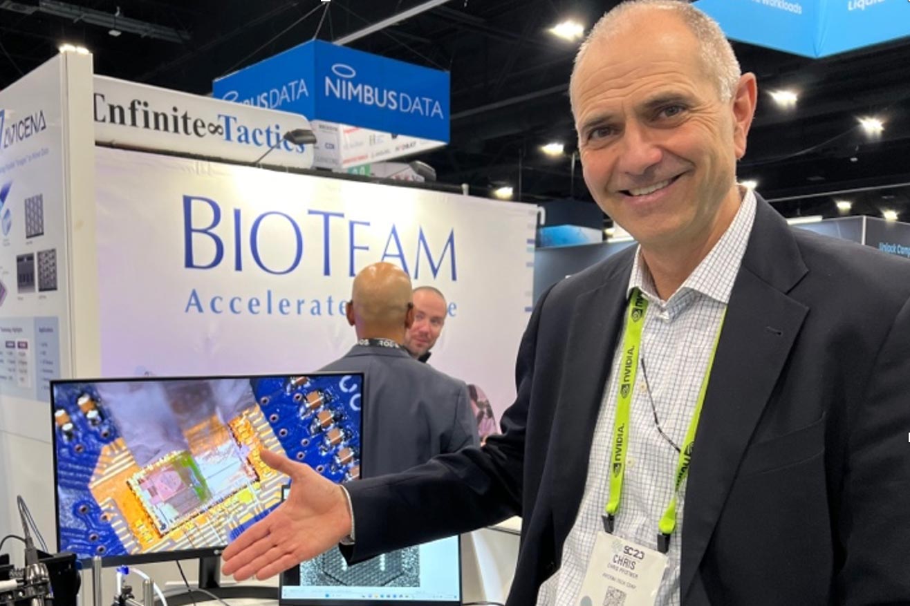
Avicena demonstrated its 1 terabit-per-second (Tbps) interface at the recent Supercomputing 23 show in Colorado last November. Its interface used 304 LED-based optical channels, each carrying 3.3 gigabit-per-second (Gbps) of data for a total bandwidth of one terabit.
The transceiver design dubbed LightBundle comprises a small 16nm CMOS process chip. Measuring 3mm x 4 mm, the chip hosts the electrical interface and the optical circuitry. These include the microLEDs, each one less that 10 microns in diameter, that emit blue light.
The LEDs are arranged in 2D arrays that are flip-chipped and bonded onto the chip. The photo-detectors are also arranged in an array and connected to the LEDs via the multimode fibres.
“On the electrical side [of the Lightbundle chip], you can put any interface you want,” says Christoph Pfistner, vice president of sales and marketing at Avicena. The ASIC uses the Open Compute Project’s OpenHBI interface for the electrical interface.
The choice of OpenHBI was due to a hyperscaler customer request. But Avicena plans to use the UCIe chiplet interface for future designs.
Performance metrics
MicroLEDs offer another category of optical interfaces alongside pluggable optical modules, on-board optics, and co-packaged optics (see chart below).
Pfistner stresses that the microLED approach is complementary and does not directly compete with silicon photonics.
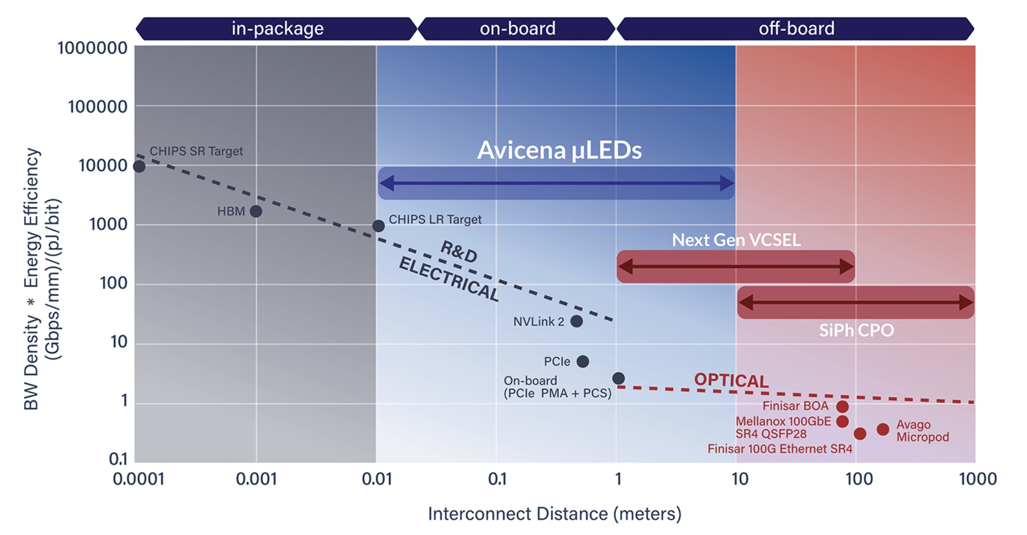
The microLEDs and multimode fibre result in a shorter reach interface – up to 10m – whereas silicon photonics interfaces cover a wider span. MicroLED technology is thus ideal for chip-to-chip applications such as interfacing graphics processor units (GPUs) with high-bandwidth memory (HBM). The microLED technology also benefits intra-rack links.
That said, Pfistner is keen to highlight the technology’s benefits. First, there is no need for an external laser source, and the link consumes fewer picoJoules-per-bit (pJ/b). Avicena says the channel consumes 1pJ/b and says its roadmap suggests sub-pJ/b interface energy consumption. Silicon photonics interfaces typically consume 3-5pJ/b, although the performance metric should also include the extranal laser source.
Like silicon photonics, the LED-based solution can send significant bandwidth across a small length of the chip’s edge, referred to as ‘beachfront’ density. Pfistner says the company can achieve more than 10Tbps/mm interface densities, with the company’s roadmap potentially going to 25Tbps/mm.
Given that this technology is multimode, there is also a relaxed tolerance – a few microns – to coupling the LED light source to the fibre bundle. This is a much more relaxed tolerance than single-mode fibre designs, which require sub-micron precision. More relaxed laser manufacturing tolerances means lower production costs.
The LED-based interface technology can also operate at over 150°C, much higher than traditional lasers. Operating temperatures up to 290°Chave been demonstrated in collaboration with Fred Kish’s North Carolina State University (NCSU) group, says Pfistner.
And since the chip supports non-return-to-zero (NRZ) signalling over short-reach spans, it has a latency advantage compared to optical interfaces requiring signal processing and error correction schemes to close links.
High bandwidth memory
Longer term, Avicena is eyeing the HBM opportunity. HBM uses stacked high-speed memory dies, with several HBMs seated around a processor IC. There is an ongoing race to stack more data in the HBM, overall memory for the processor such as GPUs, and faster data access speeds.
However, HBM has several constraints. First, only so many chips can be stacked on each other in part due to heat dissipation issues. The memory chip at the bottom of the stack must dissipate its heat through all the chips above it, and hot HBM stacks require frequent refresh cycles to retain data, which limits usable bandwidth.
One merit of HBM is that it uses a large bus – 1024 electrical channels wide, each at 6.4 Gbps (HBM3). This is ideal for Avicena’s microLED optical interface. HBM3E memory uses an even faster interface speed of 9.6Gbps. Meanwhile, HBM4, expected in a couple of years, aims to widen the electrical bus from 1024 to 2048 lanes to keep GPU designs fed with data.
Another issue is the size of the stacks relative to the large ASIC chip, such as a GPU. A finite chip size means only so many HBM can surround the ASIC. Due to space limits, high-end GPUs are limited to six HBMs, three stacks on each side of the chip.
Using an optical interface promises larger-capacity high-bandwidth memory designs where the stacks don’t have to be crammed around the ASIC. The memory can be located further away but still be accessible with low latency and energy consumption.
The ASIC-to-HBM interface is thus an important opportunity for short-reach optical interconnects. Moreover, two investors in Avicena are Samsung and Micron, leading memory suppliers.
Avicena’s is now focussed on preparing customer demo kits and increasing its yields before it ramps production for the first product, topics it will be discussing at OFC 2024.