DustPhotonics readies its first optical engine
- DustPhotonics has a silicon photonics modulator capable of 200 gigabits per lane
- The start-up also has developed a precision laser-attach scheme
Ronnen Lovinger waves as he approaches the local train station. DustPhotonics’ CEO is taking me to the company’s offices on the outskirts of Modi’in, halfway between Tel Aviv and Jerusalem.
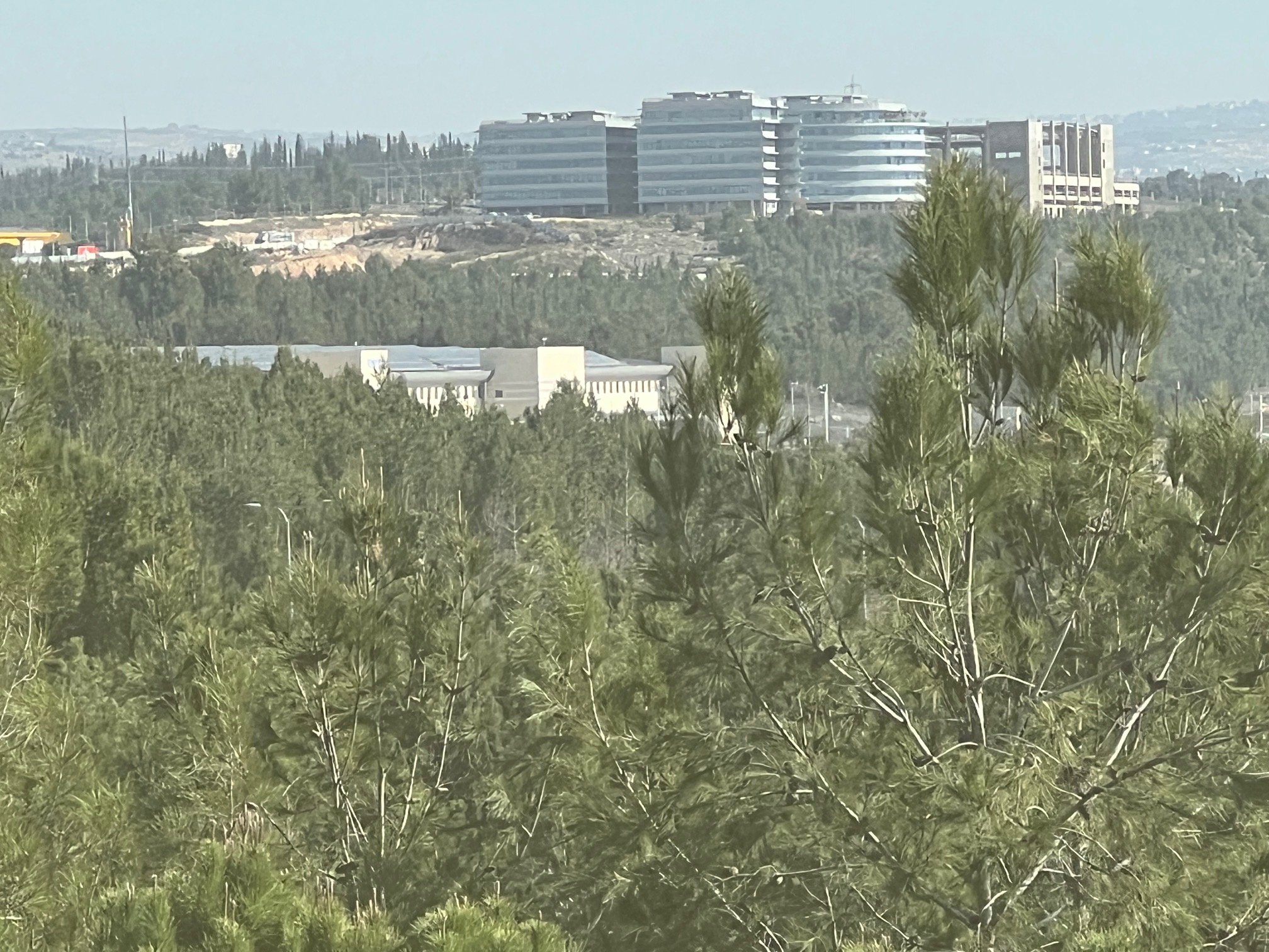
The site has a striking view of a landscape also halfway between Israel’s flat coastal plain and the steep hills of Jerusalem.
Lovinger has been CEO of DustPhotonics since 2021. Before that, he was chief operating officer (COO) at Innoviz Technologies, joining the lidar firm after 18 years at Mellanox, now part of Nvidia.
Strategic pivotStrategic pivot
DustPhotonics was founded in 2017 and has a staff of 46, 30 being R&D engineers.
The company began by developing multi-mode short-reach, up to 100m, optical transceivers and cables, first at 100 gigabits and then at 400 gigabits.
The start-up also made a single-mode transceiver using discrete components. The company planned to develop an integrated version using silicon photonics, a programme it started in 2018.
DustPhotonics gained a significant design win for its multi-mode transceiver with a customer who was to also act as its channel to market. DustPhotonics then spent two years investing in a high-volume production line in Thailand.
But the anticipated high-volume orders failed to materialise. “After those two years, we shipped 1,000s, not 100,000s of units,” says Lovinger. “It wasn’t the customer’s fault; the market where we had differentiation changed.”

DustPhotonics was forced to change tack. Instead of making modules, it decided to use its silicon photonics expertise to make optical engines.
“Silicon photonics is a very flexible platform, and you can integrate different technologies as well,” says Yoel Chetrit, CTO and vice president of R&D at DustPhotonics. “This gives us a roadmap that is not limited by the standard bandwidth restriction.”
Now the start-up has a 400-gigabit DR4 optical engine, dubbed Carmel, whose qualification is expected to be completed this month. Two DR4 engines enable an 800-gigabit DR8 that fits in an OSFP module.
Lovinger says that at the upcoming OFC show, to be held in March, the company will provide details to customers about the Carmel 8, a single-chip optical engine for 800G DR8 that is small enough to fit within a QSFP-DD module.
DustPhotonics also offers design services. The company it chooses only those projects that promise new markets and customers.
DustPhotonics’s chairman is Avigdor Willenz, a noted Israeli entrepreneur who founded Galileo Technology, was acquired by Marvell, and was chairman of such firms as Annapurna Labs, bought by Amazon, and AI chip company, Habana Labs, bought by Intel.
“He has been in the networking industry for over 30 years,” says Lovinger. “He knows how the architecture of the data centre looks now and how it will be in the future.”
Willenz also has contacts at key large companies and the hyperscalers. “He gets DustPhotonics a foot in the door,” says Lovinger.
1.6 terabit direct-detect modules
DustPhotonics is competing with much larger photonics players that have silicon photonics and indium-phosphide and can make their lasers. These players also sell optical transceivers.
Lovinger stresses that DustPhotonics has its strengths.
“Silicon photonics is a very difficult technology; the bar is very high in the expertise you need,” he says. “Many [firms] are trying, but it is difficult to get there.”
The company has developed a precision laser-attach scheme to the photonic integrated circuit (PIC) that has a sub-micron accuracy. The scheme results in the efficient coupling of light to the PIC. The company uses standard off-the-shelf continuous-wave lasers operating at 1310nm.
The efficiency of the laser attach scheme means two lasers can power an eight-channel design, reducing cost and overall power consumption, says Chetrit.
The company also has a highly stable silicon-photonics modulator that does not need to be temperature controlled and will operate at 200 gigabits per lane.
There is an ongoing industry debate as to whether direct-detect designs can meet all the reaches – 500m, 2km, and 10km – for next-generation 1.6-terabit (8x200Gbps) optical modules. If not, coherent optics will be needed.
“[Achieving] The 2km reach is really a challenge of power and the quality of the modulation,” says Chetrit. DustPhotonics says its direct-detect optical engines will support 1.6-terabit optical modules with a 2km reach.
At last year’s OFC (2022), hyperscalers wondered whether a ‘coherent-light’ design would be needed, says Lovinger: “But things have changed this year; 200 gigabit-per-lane direct detect will happen.”
Two hyperscalers have told DustPhotonics that if it can do this, it will be a game-changer.
“We looked at direct detect versus coherent, and there is no question, going to coherent is just too expensive and too power-hungry,” says Lovinger, adding that using coherent would double costs.
Status
DustPhotonics’ optical engines will be targeted at two markets. One is for pluggable module makers; the other is to supply physical layer (PHY) chip companies that also want optical engines to expand their product portfolio offerings.
The company also offers design capabilities, from photonic elements to complete products. “We don’t call ourselves an [optical] ASIC company, but it may be a similar model,” says Lovinger.
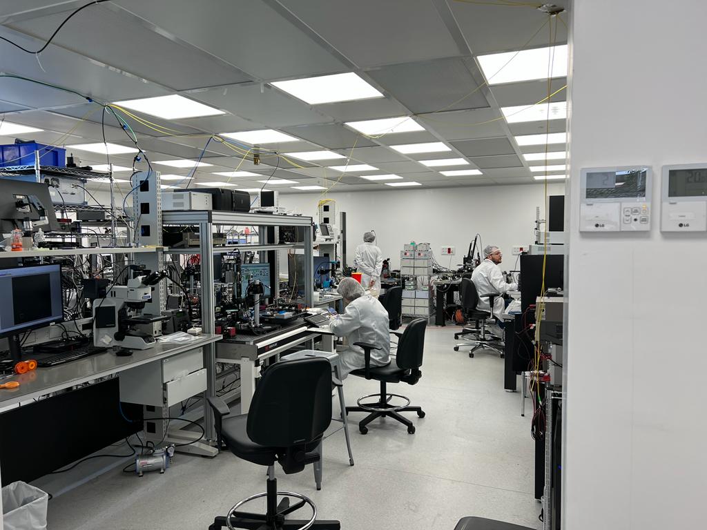
The meeting ends with a quick tour of DustPhotonics’ labs. It is here that R&D takes place, and the lab can sample build up to 1,000 optical engine products a month.
DustPhotonics recently chose Fabrinet as the outsourced assembly and test (OSAT) company. It will do the wafer dicing, burn-in, testing and packaging which will allow for production volumes much higher than in the DustPhotonics lab.
Tower Semiconductor is the silicon photonics foundry DustPhotonics is using.
“When we selected them, Tower had a mature PDK (process design kit), a very flexible process we can work with,” says Chetrit.
The industrial park where DustPhotonics is located is relatively quiet while down the road there is a much busier one. But DustPhotonics chose this one, says Lovinger, and the staff like it here. This is understandable, seeing the views from the elevated office terrace.
Lovinger then drives me to the station in time for my train to Tel Aviv and beyond.

Nokia buys Elenion for its expertise and partnerships

Nokia will become the latest systems vendor to bolster its silicon photonics expertise with the acquisition of Elenion Technologies.
The deal for Elenion, a privately-held company, is expected to be completed this quarter, subject to regulatory approval. No fee has been disclosed.
“If you look at the vertically-integrated [systems] vendors, they captured the lion’s share of the optical coherent marketplace,” says Kyle Hollasch, director of optical networking product marketing at Nokia. “But the coherent marketplace is shifting to pluggables and it is shifting to more integration; we can’t afford to be left behind.”
Elenion Technologies
Elenion started in mid-2014, with a focus of using silicon as a platform for photonics. “We consider ourselves more of a semiconductor company than an optics company,” says Larry Schwerin, CEO of Elenion.
Elenion makes photonic engines and chipsets and is not an optical module company. “We then use the embedded ecosystem to offer up solutions,” says Schwerin. “That is how we approach the marketplace.”
The company has developed a process design kit (PDK) for photonics and has built a library of circuits that it uses for its designs and custom solutions for customers.
A PDK is a semiconductor industry concept that allows circuit designers to develop complex integrated circuits without worrying about the underlying transistor physics. Adhering to the PDK ensures the circuit design is manufacturable at a chip fabrication plant (fab).
But developing a PDK for optics is tricky. How the PDK is designed and developed must be carefully thought through, as has the manufacturing process, says Elenion.

“We got started on a process and developed a library,” says Larry Schwerin, CEO of Elenion. “And we modelled ourselves on the hyperscale innovation cycle, priding ourselves that we could get down to less than three years for new products to come out.”
The “embedded ecosystem” Elenion refers to involves close relationships with companies such as Jabil to benefit from semiconductor assembly test and packaging techniques. Other partnerships include Molex and webscale player, Alibaba.
Elenion initially focussed on coherent optics, providing its CSTAR coherent device that supports 100- and 200-gigabit transmissions to Jabil for a CFP2-DCO pluggable module. Other customers also use the design, mostly for CFP2-DCO modules.
The company has now developed a third-generation coherent design, dubbed CSTAR ZR, for 400ZR optics. The optical engine can operate up to 600 gigabits-per-second (Gbps), says Elenion.
Elenion’s work with the cloud arm of Alibaba covers 400-gigabit DR4 client-side optics as well as an 800-gigabit design.
Alibaba Cloud has said the joint technology development with Elenion and Hisense Broadband covers all the production stages: the design, packaging and testing of the silicon photonics chip followed by the design, packaging, assembly and testing of the resulting optical module.
Bringing optics in-house
With the acquisition of Elenion, Nokia becomes the latest systems vendors to buy a silicon photonics specialist.
Cisco Systems acquired Lightwire in 2012 that enabled it to launch the CPAK, a 100-gigabit optical module, a year ahead of its rivals. Cisco went on another silicon photonics shopping spree more recently with the acquisition of Luxtera in 2019, and it is the process of acquiring leading merchant coherent player, Acacia Communications.
In 2013 Huawei bought the Belgium silicon photonics start-up, Caliopa, while Mellanox Technologies acquired silicon photonics firm, Kotura, although subsequently, it disbanded its silicon photonics arm.
Ciena bought the silicon-photonics arm of Teraxion in 2016 and, in the same year, Juniper bought silicon photonics start-up, Aurrion Technologies.
Markets
Nokia highlights several markets – 5G, cloud and data centres – where optics is undergoing rapid change and where the system vendor’s designs will benefit from Elenion’s expertise.
“5G is a pretty obvious one; a significant portion of our optical business over the last two years has been mobile front-haul,” says Nokia’s Hollasch. “And that is only going to become more significant with 5G.”
Front-haul is optics-dependent and requires new pluggable form factors supporting lower data rates such as 25Gbps and 100Gbps. “This is the new frontier for coherent,” says Hollasch.
Nokia is not looking to be an optical module provider, at least for now. “That one we are treading cautiously,” says Hollasch. “We, ourselves, are quite a massive customer [of optics] which gives us some built-in scale straight away but our go-to-market [strategy] is still to be determined.”
Not being a module provider, adds Schwerin, means that Nokia doesn’t have to come out with modules to capitalise on what Elenion has been doing.
Nokia says both silicon photonics and indium phosphide will play a role for its coherent optical designs. Nokia also has its own coherent digital signal processors (DSPs).
“There is an increasingly widening application space for silicon photonics,” says Hollasch. “Initially, silicon photonics was looked at for the data centre and then strictly for metro [networks]; I don’t think that is the case anymore.”
Why sell?
Schwerin says the company was pragmatic when it came to being sold. Elenion wasn’t looking to be acquired and the idea of a deal came from Nokia. But once the dialogue started, the deal took shape.
“The industry is in a tumultuous state and from a standpoint of scenario planning, there are multiple dynamics afoot,” says Schwerin.
As the company has grown and started working with larger players including webscales, their requirements have become more demanding.
“As you get more into bigs, they require big,” says Schwerin. “They want supply assurance, and network indemnification clauses come into play.” The need to innovate is also constant and that means continual investment.
“When you weigh it all up, this deal makes sense,” he says.
Schwerin laughs when asked what he plans to do next: “I know what my wife wants me to do.
“I will be going with this organisation for a short while at least,” he says. “You have to make sure things go well in the absorption process involving big companies and little companies.”

Inphi adds a laser driver to its 100-gigabit PAM-4 DSP
Inphi has detailed its second-generation Porrima chip family for 100-gigabit single-wavelength optical module designs.

Source: Inphi
The Porrima family of devices is targeted at the 400G DR4 and 400G FR4 specifications as well as 100-gigabit module designs that use 100-gigabit 4-level pulse-amplitude modulation (PAM-4). Indeed, the two module types can be combined when a 400-gigabit pluggable such as a QSFP-DD or an OSFP is used in breakout mode to feed four 100-gigabit modules using such form factors as the QSFP, uQSFP or SFP-DD.
The Gen2 family has been launched a year after the company first announced the Porrima. The original 400-gigabit and 100-gigabit Porrima designs each have three ICs: a PAM-4 digital signal processor (DSP), a trans-impedance amplifier (TIA) and a laser-driver.
“With Gen2, the DSP and laser driver are integrated into a single monolithic CMOS chip, and there is a separate amplifier chip,” says Siddharth Sheth, senior vice president, networking interconnect at Inphi. The benefit of integrating the laser driver with the DSP is lower cost, says Sheth, as well as a power consumption saving.
The second-generation Porrima family is now sampling with general availability expected in mid-2019.
PAM-4 families
Inphi has three families of PAM-4 ICs targeting 400-gigabit interfaces: the Polaris, Vega and Porrima.
The Polaris, Inphi’s first product family, uses a 200-gigabit die and two are used within the same package for 400-gigabit module designs. As well as the PAM-4 DSP, the Polaris family also comprises two companion chips: a laser driver and an amplifier.
Inphi’s second family is the Vega, a 8x50-gigabit PAM-4 400-gigabit DSP chip that sits on a platform’s line card.
“The chip is used to drive backplanes and copper cables and can be used as a retimer chip,” says Sheth.

Siddharth Sheth
“For the Porrima family, you have a variant that does 4x100-gigabit and a variant that does 1x100-gigabit,” says Sheth. The Porrima can interface to a switch chip that uses either 4x25-gigabit non-return-to-zero (NRZ) or 2x50-gigabit PAM-4 electrical signals.
Why come out with a Gen2 design only a year after the first Porrima? Sheth says there was already demand for 400-gigabit PAM-4 chips when the Porrima first became available in March 2018. Optical module makers needed such chips to come to market with 400-gigabit modules to meet the demand of an early hyperscale data centre operator.
“Now, the Gen2 solution is for the second wave of customers,” says Sheth. “There are going to be two or three hyperscalers coming online in 2020 but maybe not as aggressively as the first hyperscaler.” These hyperscalers will be assessing the next generation of 400-gigabit PAM-4 silicon available, he says.
The latest design, like the first generation Porrima, is implemented using 16nm CMOS. The DSP itself has not been modified; what has been added is the laser-driver circuitry. Accordingly, it is the transmitter side that has been changed, not the receiver path where Inphi does the bulk of the signal processing. “We did not want to change a whole lot because that would require a change to the software,” he says.
A 400-gigabit optical module design using the first generation Porrima consumes under 10W but only 9W using the Gen2. The power saving is due to the CMOS-based laser driver consuming 400mW only compared to a gallium arsenide or silicon germanium-based driver IC that consumes between 1.6W to 2W, says Inphi.
The internal driver can achieve transmission distances of 500m while a standalone driver will still be needed for longer 2km spans.
Sheth says that the advent of mature low-swing-voltage lasers will mean that the DSP’s internal driver will also support 2km links.
PAM-4 DSP
The aim of the DSP chip is to recover the transmitted PAM-4 signal. Sheth says PAM-4 chip companies differ in how much signal processing they undertake at the transmitter and how much is performed at the receiver.
“It comes down to a tradeoff, we believe that we are better off putting the heavier signal processing on the receive side,” says Sheth.
Inphi performs some signal processing on the transit side where transmit equalisation circuits are used in the digital domain, prior to the digital-to-analogue converter.
The goal of the transmitter is to emit a signal with the right amplitude, pre-emphasis, and having a symmetrical rise and fall. But even generating such a signal, the PAM-4 signal recovered at the receiver may look nothing like the signal sent due to degradations introduced by the channel. “So we have to do all kind of tricks,” he says.
Inphi uses a hybrid approach at the receiver where some of the signal processing is performed in the analogue domain and the rest digitally. A variable-gain amplifier is used up front to make sure the received signal is at the right amplitude and then feed-forward equalisation is performed. After the analogue-to-digital stage, post equalisation is performed digitally.
Sheth says that depending on the state of the received signal - the distortion, jitter and loss characteristics it has - different functions of the DSP may be employed.
One such DSP function is a reflection canceller that is turned on, depending on how much signal reflection and crosstalk occur. Another functional block that can be employed is a maximum likelihood sequence estimator (MLSE) used to recover a signal sent over longer distances. In addition, forward-error correction blocks can also be used to achieve longer spans.
“We have all sorts of knobs built into the chip to get an error-free link with really good performance,” says Sheth. “At the end of the day, it is about closing the optical link with plenty of margin.”
What next?
Sheth says the next-generation PAM-4 design will likely use an improved DSP implemented using a more advanced CMOS process.
“We will take the learning from Gen1 and Gen2 and roll it into a ‘Gen3’,” says Sheth.
Such a design will also be implemented using a 7nm CMOS process. “We are now done with 16nm CMOS,” concludes Sheth.