
Inphi adds a laser driver to its 100-gigabit PAM-4 DSP
Inphi has detailed its second-generation Porrima chip family for 100-gigabit single-wavelength optical module designs.

Source: Inphi
The Porrima family of devices is targeted at the 400G DR4 and 400G FR4 specifications as well as 100-gigabit module designs that use 100-gigabit 4-level pulse-amplitude modulation (PAM-4). Indeed, the two module types can be combined when a 400-gigabit pluggable such as a QSFP-DD or an OSFP is used in breakout mode to feed four 100-gigabit modules using such form factors as the QSFP, uQSFP or SFP-DD.
The Gen2 family has been launched a year after the company first announced the Porrima. The original 400-gigabit and 100-gigabit Porrima designs each have three ICs: a PAM-4 digital signal processor (DSP), a trans-impedance amplifier (TIA) and a laser-driver.
“With Gen2, the DSP and laser driver are integrated into a single monolithic CMOS chip, and there is a separate amplifier chip,” says Siddharth Sheth, senior vice president, networking interconnect at Inphi. The benefit of integrating the laser driver with the DSP is lower cost, says Sheth, as well as a power consumption saving.
The second-generation Porrima family is now sampling with general availability expected in mid-2019.
PAM-4 families
Inphi has three families of PAM-4 ICs targeting 400-gigabit interfaces: the Polaris, Vega and Porrima.
The Polaris, Inphi’s first product family, uses a 200-gigabit die and two are used within the same package for 400-gigabit module designs. As well as the PAM-4 DSP, the Polaris family also comprises two companion chips: a laser driver and an amplifier.
Inphi’s second family is the Vega, a 8x50-gigabit PAM-4 400-gigabit DSP chip that sits on a platform’s line card.
“The chip is used to drive backplanes and copper cables and can be used as a retimer chip,” says Sheth.

Siddharth Sheth
“For the Porrima family, you have a variant that does 4x100-gigabit and a variant that does 1x100-gigabit,” says Sheth. The Porrima can interface to a switch chip that uses either 4x25-gigabit non-return-to-zero (NRZ) or 2x50-gigabit PAM-4 electrical signals.
Why come out with a Gen2 design only a year after the first Porrima? Sheth says there was already demand for 400-gigabit PAM-4 chips when the Porrima first became available in March 2018. Optical module makers needed such chips to come to market with 400-gigabit modules to meet the demand of an early hyperscale data centre operator.
“Now, the Gen2 solution is for the second wave of customers,” says Sheth. “There are going to be two or three hyperscalers coming online in 2020 but maybe not as aggressively as the first hyperscaler.” These hyperscalers will be assessing the next generation of 400-gigabit PAM-4 silicon available, he says.
The latest design, like the first generation Porrima, is implemented using 16nm CMOS. The DSP itself has not been modified; what has been added is the laser-driver circuitry. Accordingly, it is the transmitter side that has been changed, not the receiver path where Inphi does the bulk of the signal processing. “We did not want to change a whole lot because that would require a change to the software,” he says.
A 400-gigabit optical module design using the first generation Porrima consumes under 10W but only 9W using the Gen2. The power saving is due to the CMOS-based laser driver consuming 400mW only compared to a gallium arsenide or silicon germanium-based driver IC that consumes between 1.6W to 2W, says Inphi.
The internal driver can achieve transmission distances of 500m while a standalone driver will still be needed for longer 2km spans.
Sheth says that the advent of mature low-swing-voltage lasers will mean that the DSP’s internal driver will also support 2km links.
PAM-4 DSP
The aim of the DSP chip is to recover the transmitted PAM-4 signal. Sheth says PAM-4 chip companies differ in how much signal processing they undertake at the transmitter and how much is performed at the receiver.
“It comes down to a tradeoff, we believe that we are better off putting the heavier signal processing on the receive side,” says Sheth.
Inphi performs some signal processing on the transit side where transmit equalisation circuits are used in the digital domain, prior to the digital-to-analogue converter.
The goal of the transmitter is to emit a signal with the right amplitude, pre-emphasis, and having a symmetrical rise and fall. But even generating such a signal, the PAM-4 signal recovered at the receiver may look nothing like the signal sent due to degradations introduced by the channel. “So we have to do all kind of tricks,” he says.
Inphi uses a hybrid approach at the receiver where some of the signal processing is performed in the analogue domain and the rest digitally. A variable-gain amplifier is used up front to make sure the received signal is at the right amplitude and then feed-forward equalisation is performed. After the analogue-to-digital stage, post equalisation is performed digitally.
Sheth says that depending on the state of the received signal - the distortion, jitter and loss characteristics it has - different functions of the DSP may be employed.
One such DSP function is a reflection canceller that is turned on, depending on how much signal reflection and crosstalk occur. Another functional block that can be employed is a maximum likelihood sequence estimator (MLSE) used to recover a signal sent over longer distances. In addition, forward-error correction blocks can also be used to achieve longer spans.
“We have all sorts of knobs built into the chip to get an error-free link with really good performance,” says Sheth. “At the end of the day, it is about closing the optical link with plenty of margin.”
What next?
Sheth says the next-generation PAM-4 design will likely use an improved DSP implemented using a more advanced CMOS process.
“We will take the learning from Gen1 and Gen2 and roll it into a ‘Gen3’,” says Sheth.
Such a design will also be implemented using a 7nm CMOS process. “We are now done with 16nm CMOS,” concludes Sheth.

Rockley Photonics eyes multiple markets
Andrew Rickman, founder and CEO of silicon photonics start-up, Rockley Photonics, discusses the new joint venture with Hengtong Optic-Electric, the benefits of the company’s micron-wide optical waveguides and why the timing is right for silicon photonics.
 Andrew Rickman
The joint venture between Rockley Photonics and Chinese firm Hengtong Optic-Electric is the first announced example of Rockley’s business branching out.
The start-up’s focus has been to apply its silicon photonics know-how to data-centre applications. In particular, Rockley has developed an Opto-ASIC package that combines optical transceiver technology with its own switch chip design. Now it is using the transceiver technology for its joint venture.
“It was logical for us to carve out the pieces generated for the Opto-ASIC and additionally commercialise them in a standard transceiver format,” says Andrew Rickman, Rockley’s CEO. “That is what the joint venture is all about.”
Rockley is not stopping there. Rickman describes the start-up as a platform business, building silicon photonics and electronics chipsets for particular applications including markets other than telecom and datacom.
Joint venture
Hengtong and Rockley have set up the $42 million joint venture to make and sell optical transceivers.
Known for its optical fibre cables, Hengtong is also a maker of optical transceivers and owns 75.1 percent of the new joint venture. Rockley gains the remaining 24.9 percent share in return for giving Hengtong its 100-gigabit QSFP transceiver designs. The joint venture also becomes a customer of Rockley’s, buying its silicon photonics and electronics chips to make the QSFP modules.
“Hengtong is one of the world’s largest optical fibre cable manufacturers, is listed on the Shanghai stock market, and sells extensively in China and elsewhere into the data centre market,” says Rickman. “It is a great conduit, a great sales channel into these customers.”
The joint venture will make three 100-gigabit QSFP-based products: a PSM4 and a CWDM4 pluggable module and an active optical cable. Rickman expects the joint venture to make other module designs and points out that Rockley participates in the IEEE standards work for 400 gigabits and is one of the co-founders of the 400-gigabit CWDM8 MSA.
Rockley cites several reasons why the deal with Hengtong makes sense. First, a large part of the bill of materials used for active optical cables is the fibre itself, something which the vertically integrated Hengtong can provide.
China also has a ‘Made in China 2025’ initiative that encourages buying home-made optical modules. Teaming with Hengtong means Rockley can sell to the Chinese telecom operators and internet content players.
In addition, Hengtong is already doing substantial business with all of the global data centres as a cable, patch panel and connector supplier, says Rickman:“So it is an immediate sales channel into these companies without having to break into these businesses as a qualified supplier afresh.”
A huge amount of learning happened and then what Rockley represented was the opportunity to start all over again with a clean sheet of paper but with all that experience
Bigger is Best?
At the recent SPIE Photonics West conference held in San Francisco, Rickman gave a presentation entitled Silicon Photonics: Bigger is Better. His talk outlined the advantages of Rockley’s use of three-micron-wide optical waveguides, bucking the industry trend of using relatively advanced CMOS processes to make silicon photonics components.
Rickman describes as seductive the idea of using 45nm CMOS for optical waveguides.“These things exist and work but people are thinking of them in the same physics that have driven microelectronics,” he says. Moving to ever-smaller feature sizes may have driven Moore’s Law but using waveguide dimensions that are smaller than the wavelength of light makes things trickier.
To make his point, he plots the effective index of a waveguide against its size in microns. The effective index is a unitless measure - a ratio of a phase delay in a unit length of a waveguide relative to the phase delay in a vacuum. “Once you get below one micron, you get a waveguide that is highly polarisation-dependent and just a small variation in the size of the waveguide has a huge variation in the effective index,” says Rickman.
Such variations translate to inaccuracies in the operating wavelength. This impacts the accuracy of circuits, for example, arrayed-waveguide gratings built using waveguides to multiplex and demultiplex light for wavelength-division multiplexing (WDM).
“Above one micron is where you want to operate, where you can manufacture with a few percent variation in the width and height of a waveguide,” says Rickman.“But the minute you go below one micron, in order to hit the wavelength registration that you need for WDM, you have got to control the [waveguide’s] film thickness and line thickness to fractions of a percent.” A level of accuracy that the semiconductor industry cannot match, he says.
A 100GHz WDM channel equates to 0.8nm when expressed using a wavelength scale. “In our technology, you can easily get a wavelength registration on a WDM grid of less than 0.1nm,” says Rickman. “Exactly the same manufacturing technology applied to smaller waveguides is 25 times worse - the variation is 2.5nm.”
Moreover, WDM technology is becoming increasingly important in the data centre. The 100-gigabit PSM4 uses a single wavelength, the CWDM4 uses four, while the newer CWDM8 MSA for 400 gigabit uses eight wavelengths. “In telecom, 90-plus wavelengths can be used; the same thing will come to pass in the years to come in data centre devices,” he says.
Rockley also claims it has a compact modulator that is 50 times smaller than competing modulators despite them being implemented using nanometer feature sizes.
We set out to generate a platform that would be pervasive across communications, new forms of advanced computing, optical signal processing and a whole range of sensor applications
Opto-ASIC reference design
Rockley’s first platform technology example is its Opto-ASIC reference design. The design integrates silicon photonics-based transceivers with an in-house 2 billion transistor switch chip all in one package. Rockley demonstrated the technology at OFC 2017.
“If you look around, this is something the industry says is going to happen but there isn't a single practical instantiation of it,” says Rickman who points out that, like the semiconductor industry, very often a reference design needs to be built to demonstrate the technology to customers.“So we built a complete reference design - it is called Topanga - an optical-packaged switch solution,” he says.
Despite developing a terabyte-class packet processor, Rockley does not intend to compete with the established switch-chip players. The investment needed to produce a leading edge device and remain relevant is simply too great, he says.
Rockley has demonstrated its in-package design to relevant companies. “It is going very well but nothing we can say publicly,” says Rickman.
New Markets
Rockley is also pursuing opportunities beyond telecom and datacom.
“We set out to generate a platform that would be pervasive across communications, new forms of advanced computing, optical signal processing and a whole range of sensor applications,” says Rickman.
Using silicon photonics for sensors is generating a lot of interest. “We see these markets starting to emerge and they are larger than the data centre and communications markets,” he says. “A lot of these things are not in the public domain so it is very difficult to report on.”
Moreover, the company’s believes its technology gives it an advantage for such applications. “When we look across the other application areas, we don’t see the small waveguide platforms being able to compete,” says Rickman. Such applications can use relatively high power levels that exceed what the smaller waveguides can handle.
Rockley is sequencing the markets it will address. “We’ve chosen an approach where we have looked at the best match of the platform to the best opportunities and put them in an order that makes sense,” says Rickman.
Rockley Photonics represent Rickman’s third effort to bring silicon photonics to the marketplace.Bookham Technology, the first company he founded, build different prototypes in several different areas but the market wasn't ready. In 2005 he joined start-up Kotura as a board member. “A huge amount of learning happened and then what Rockley represented was the opportunity to start all over again with a clean sheet of paper but with all that experience,” says Rickman.
Back in 2013, Rockley saw certain opportunities for its platform approach and what has happened since is that their maturity and relevance has increased dramatically.
“Like all things it is always down to timing,” says Rickman. “The market is vastly bigger and much more ready than it was in the Bookham days.”
Verizon, Ciena and Juniper trial 400 Gigabit Ethernet
Verizon has sent a 400 Gigabit Ethernet signal over its network, carried using a 400-gigabit optical wavelength.
The trial’s goal was to demonstrate multi-vendor interoperability and in particular the interoperability of standardised 400 Gigabit Ethernet (GbE) client signals.
 Glenn Wellbrock“[400GbE] Interoperability with the client side has been the long pole in the tent - and continues to be,” says Glenn Wellbrock, director, optical transport network - architecture, design and planning at Verizon. “This was trial equipment, not generally-available equipment.”
It is only the emergence of standardised modules - in this case, an IEEE 400GbE client-side interface specification - that allows multi-vendor interoperability, he says.
By trialing a 400-gigabit lightpath, Verizon also demonstrated the working of a dense wavelength-division multiplexing (DWDM) flexible grid, and a baud rate nearly double the 32-35Gbaud in wide use for 100-gigabit and 200-gigabit wavelengths.
“It shows we can take advantage of the entire system; we don’t have to stick to 50GHz channel spacing anymore,” says Wellbrock.
[400GbE] Interoperability with the client side has been the long pole in the tent - and continues to be
Trial set-up
The trial used Juniper Networks’ PTX5000 packet transport router and Ciena’s 6500 packet-optical platform, equipment already deployed in Verizon’s network.
The Verizon demonstration was not testing optical transmission reach. Indeed the equipment was located in two buildings in Richardson, within the Dallas area. Testing the reach of 400-gigabit wavelengths will come in future trials, says Wellbrock.
The PTX5000 core router has a traffic capacity of up to 24 terabits and supports 10-gigabit, 40-gigabit and 100-gigabit client-side interfaces as well as 100-gigabit coherent interfaces for IP-over-DWDM applications. The PTX5000 uses a mother card on which sits one or more daughter cards hosting the interfaces, what Juniper calls a flexible PIC concentrator (FPC) and physical interface cards (PICs), respectively.
Juniper created a PIC with a 400GbE CFP8 pluggable module implementing the IEEE’s 10km 400GBASE-LR8 standard.
“For us, it was simply creating a demo 400-gigabit pluggable line card to go into the line card Verizon has already deployed,” says Donyel Jones-Williams, director of product marketing management at Juniper Networks.
 Donyel Jones-WilliamsThe CFP8 400GbE interface connected the router to Ciena’s 6500 packet-optical platform.
Ciena also used demonstration hardware developed for 400-gigabit trials. “We expect to develop other hardware for general deployment,” says Helen Xenos, senior director, portfolio marketing at Ciena. “We are looking at smaller form-factor pluggables to carry 400 Gigabit Ethernet.”
400-gigabit deployments and trials
Ciena started shipping its WaveLogic Ai coherent modem that implements 400-gigabit wavelengths in the third quarter of 2017. Since then, the company has announced several 400-gigabit deployments and trials.
Vodafone New Zealand deployed 400 gigabits in its national transport network last September, a world first, claims Ciena. German cable operator, Unitymedia, has also deployed Ciena’s WaveLogic Ai coherent modem to deliver a flexible grid and 400-gigabit wavelengths to support growing content delivered via its data centres. And JISC, which runs the UK’s national research and education network, has deployed the 6500 platform and is using 400-gigabit wavelengths.
 Helen Xenos
Last September, AT&T conducted its own 400-gigabit trial with Ciena. With AT&T’s trial, the 400-gigabit signal was generated using a test bed. “An SDN controller was used to provision the circuit and the [400-gigabit] signal traversed an OpenROADM line system,” says Xenos.
Using the WaveLogic Ai coherent modem and its support for a 56Gbaud rate means that tunable capacity can now be doubled across applications, says Xenos. The wavelength capacity used for long-haul distances can now be 200 gigabits instead of 100 gigabits, while metro-regional networks spanning 1,000km can use 300-gigabit wavelengths. Meanwhile, 400-gigabit lightpaths suit distances of several hundred kilometres.
It is the large data centre operators that are driving the majority of 400 gigabit deployments, says Ciena. The reason the 400-gigabit announcements relate to telecom operators is because the data centre players have not gone public with their deployments, says Xenos.
Juniper Networks’ PTX5000 core router with 400GbE interfaces will primarily be used by the telecom operators. “We are in trials with other providers on 400 gigabits,” says Jones-Williams. “Nothing is public as yet.”
Acacia announces a 1.2 terabit coherent module
 Channel capacity and link margin can be maximised by using the fractional QAM scheme. Source: Acacia.
The company is facing increasing market competition. Ciena has teamed up with Lumentum, NeoPhotonics, and Oclaro, sharing its high-end coherent DSP expertise with the three optical module makers. Meanwhile, Inphi has started sampling its 16nm CMOS M200, a 100- and 200-gigabit coherent DSP suitable for CFP2-ACO, CFP-DCO, and CFP2-DCO module designs.
The AC1200 is Acacia’s response, extending its high-end module offering beyond a terabit to compete with the in-house system vendors and preserve its performance lead against the optical module makers.
Enhanced coherent techniques
The AC1200 has an architecture similar to the company’s AC400 5x7-inch 400-gigabit module announced in 2015. Like the earlier module, the AC1200 features a dual-core coherent DSP and two silicon photonics transceiver chips. But the AC1200 uses a much more sophisticated DSP - the 16nm CMOS Pico device announced earlier this year - capable of supporting such techniques as variable baud rate, advanced modulation and coding schemes so that the bits per symbol can be fine-tuned, and enhanced soft-decision forward error correction (SD-FEC). The AC400 uses the 1.3 billion transistor Denali dual-core DSP while the Pico DSP has more than 2.5 billion transistors.
The result is a two-wavelength module design, each wavelength supporting from 100-600 gigabits in 50-gigabit increments.
Acacia is able to triple the module’s capacity to 1.2 terabits by incorporating a variable baud rate up to at least 69 gigabaud (Gbaud). This doubles the capacity per wavelength compared to the AC400 module. The company also uses more modulation formats including 64-ary quadrature amplitude modulation (64-QAM), boosting capacity a further 1.5x compared to the AC400’s 16-QAM.
Acacia has not detailed the module’s dimensions but says it is a custom design some 40 percent smaller in area than a 5x7-inch module. Nor will it disclose the connector type and electrical interface used to enable the 1.2-terabit throughput. However, the AC1200 will likely support 50 gigabit-per-second (Gbps) 4-level pulse-amplitude modulation (PAM-4) electrical signals as it will interface to 400-gigabit client-side modules such as the QSFP-DD.
The AC1200’s tunable baud rate range is around 35Gbaud to 69Gbaud. “The clock design and the optics could truly be continuous and it [the baud rate] pairs with a matrix of modulation formats to define a certain resolution,” says Tom Williams, senior director of marketing at Acacia Communications. Whereas several of the system vendors’ current in-house coherent DSPs use two baud rates such as 33 and 45Gbaud, or 35 and 56Gbaud, Acacia says it uses many more rates than just two or three.
The result is that at the extremes, the module can deliver from 100 gigabits (a single wavelength at some 34Gbaud and quadrature phase-shift keying - QPSK) to 1.2 terabits (using two wavelengths, each 64-QAM at around 69Gbaud).
The module also employs what Acacia refers to as very fine resolution QAM constellations. The scheme enables the number of bits per symbol to be set to any value and not be limited to integer bits. Acacia is not saying how it is implementing this but says the end result is similar to probabilistic shaping. “Instead of 2 or 3 bits-per-symbol, you can be at 2.5 or 2.7 bits-per-symbol,” says Williams. The performance benefits include maximising the link margin and the capacity transmitted over a given link. (See diagram, top.)
The SD-FEC has also been strengthened to achieve a higher coding gain while still being a relatively low-power implementation.
 Using a higher baud rate allows a lower order modulation scheme to be used. This can more than double the reach. Source: Acacia
The company says it is restricted in detailing the AC1200’s exact performance. “Because we are a merchant supplier selling into system vendors that do the link implementations, we have to be careful about the reach expectations we set,” says Williams. But the combination of fractional QAM, a tunable baud rate, and improved FEC means a longer reach for a given capacity. And the capacity can be tuned in 50-gigabit increments.
Platforms and status
ADVA Optical Networking is one vendor that has said it is using Acacia’s 1.2-terabit design for its Teraflex product, the latest addition to its CloudConnect family of data centre interconnect products.
Is ADVA Optical Networking using the AC1200? “Our TeraFlex data centre interconnect product uses a coherent engine specifically developed to meet the performance expectations that our customers demand,” says ADVA's spokesperson.
Teraflex is a one-rack-unit (1RU) stackable chassis that supports three hot-pluggable 1.2-terabit ‘sleds’. Each sled’s front panel supports various client-side interface module options: 12 x 100-gigabit QSFP28s, 3 x 400-gigabit QSFP-DDs and lower speed 10-gigabit and 40-gigabit modules using ADVA Optical Networking’s MicroMux technology.
Samples of the AC1200 module will be available in the first half of 2018, says Acacia. General availability will likely follow a quarter or two later.
MultiPhy unveils 100G single-wavelength PAM-4 chip
A chip to enable 100-gigabit single-wavelength client-side optical modules has been unveiled by MultiPhy. The 100-gigabit 4-level pulse amplitude modulation (PAM-4) circuit will also be a key building block for 400 Gigabit Ethernet interfaces that use four wavelengths.
 Source: MultiPhy
Dubbed the MPF3101, the 100-gigabit physical layer (PHY) chip is aimed at such applications as connecting switches within data centres and for 5G cloud radio access network (CRAN).
“The chip has already been sent out to customers and we are heading towards market introductions,” says Avi Shabtai, CEO of MultiPhy.
The MPF3101 will support 100-gigabit over 500m, 2km and 10km.
The IEEE has developed the 100-gigabit 100GBASE-DR standard for 500m while the newly formed 100G Lambda MSA (multi-source agreement) is developing specifications for the 2km 100-gigabit single-channel 100G-FR and the 10km 100G-LR.
MultiPhy says the QSFP28 will be the first pluggable module to implement a 100-gigabit single-wavelength design using its chip. The SFP-DD MSA, currently under development, will be another pluggable form factor for the single-wavelength 100-gigabit designs.
The chip has already been sent out to customers and we are heading towards market introductions
400 Gigabit
The 100-gigabit IP will also be a key building block for a second MultiPhy chip for 400-gigabit optical modules needed for next-generation data centre switches that have 6.4 and 12.8 terabits of capacity. “This is the core engine for all these markets,” says Shabtai.
Companies have differing views as to how best to address the 400-gigabit interconnect market. There is a choice of form factors such as the OSFP, QSFP-DD and embedded optics based on the COBO specification, as well as emerging standards and MSAs.
The dilemma facing companies is what approach will deliver 400-gigabit modules to coincide with the emergence of next-generation data centre switches.
One consideration is the technical risk associated with implementing a particular design. Another is cost, with the assumption that 4-wavelength 400-gigabit designs will be cheaper than 8x50-gigabit based modules but that they may take longer to come to market.
For 400 gigabits, the IEEE 803.3bs 400 Gigabit Ethernet Task Force has specified the 400GBASE-DR4, a 500m-reach four-wavelength specification that uses four parallel single-mode fibres. The 100G Lambda MSA is also working on a 400-gigabit 2km specification based on coarse wavelength-division multiplexing (CWDM), known as 400G-FR4, with work on a 10km reach specification to start in 2018.
We are hearing a lot in the industry about 50-gigabit-per-lambda. For us, this is old news; we are moving to 100-gigabit-per-lambda and we believe the industry will align with us.
And at ECOC 2017 show, held last week in Gothenburg, another initiative - the CWDM8 MSA - was announced. The CWDM8 is an alternative design to the IEEE specifications that sends eight 50-gigabit non-return-to-zero signals rather that PAM-4 over a fibre.
“We are hearing a lot in the industry about 50-gigabit-per-lambda,” says Shabtai. “For us, this is old news; we are moving to 100-gigabit-per-lambda and we believe the industry will align with us.”
Chip architecture
The MPF3101, implemented using a 16nm CMOS process, supports PAM-4 at symbol rates up to 58 gigabaud.
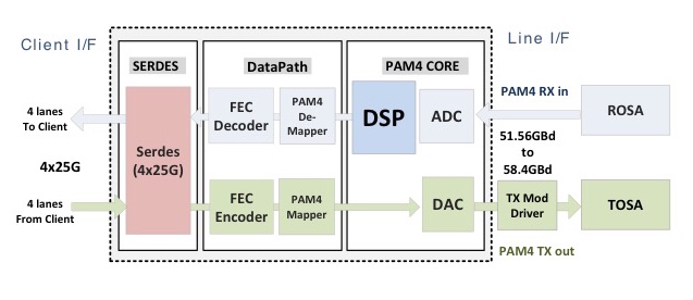
The chip’s electrical input is four 25-gigabit lanes that are multiplexed and encoded into a 50-plus gigabaud PAM-4 signal that is fed to a modulator driver, part of a 100-gigabit single-channel transmitter optical sub-assembly (TOSA). A 100-gigabit receiver optical sub-assembly (ROSA) feeds the received PAM-4 encoded signal to the chip’s DSP before converting the 100-gigabit signal to 4x25 gigabit electrical signals (see diagram).
“If you need now only one laser and one optical path [for 100 gigabits] instead of four [25 gigabits optical paths], that creates a significant cost reduction,” says Shabtai.
The advent of a single-wavelength 100-gigabit module promises several advantages to the industry. One is lower cost. Estimates that MultiPhy is hearing is that a single-wavelength 100-gigabit module will be half the cost of existing 4x25-gigabit optical modules. Such modules will also enable higher-capacity switches as well as 100-gigabit breakout channels when connected to a 400-gigabit four-wavelength module. Lastly, MultiPhy expects the overall power consumption to be less.
Availability
MultiPhy says first 100-gigabit single-wavelength QSFP28s will appear sometime in 2018.
The company is being coy as to when it will have a 400-gigabit PAM-4 chip but it points out that by having working MPF3101 silicon, it is now an integration issue to deliver a 4-channel 400-gigabit design.
As for the overall market, new high-capacity switches using 400-gigabit modules will start to appear next year. The sooner four-channel 400-gigabit PAM-4 silicon and optical modules appear, the less opportunity there will be for eight-wavelength 400-gigabit designs to gain a market foothold.
“That is the race we are in,” says Shabtai.
The OIF’s 400ZR coherent interface starts to take shape
Part 2: Coherent developments
The Optical Internetworking Forum’s (OIF) group tasked with developing two styles of 400-gigabit coherent interface is now concentrating its efforts on one of the two.
When first announced last November, the 400ZR project planned to define a dense wavelength-division multiplexing (DWDM) 400-gigabit interface and a single wavelength one. Now the work is concentrating on the DWDM interface, with the single-channel interface deemed secondary.
 Karl Gass"It [the single channel] appears to be a very small percentage of what the fielded units would be,” says Karl Gass of Qorvo and the OIF Physical and Link Layer working group vice chair, optical, the group responsible for the 400ZR work.
The likelihood is that the resulting optical module will serve both applications. “Realistically, probably both [interfaces] will use a tunable laser because the goal is to have the same hardware,” says Gass.
The resulting module may also only have a reach of 80km, shorter than the original goal of up to 120km, due to the challenging optical link budget.
Origins and status
The 400ZR project began after Microsoft and other large-scale data centre players such as Google and Facebook approached the OIF to develop an interoperable 400-gigabit coherent interface they could then buy from multiple optical module makers.
The internet content providers’ interest in an 80km-plus link is to connect premises across the metro. “Eighty kilometres is the magic number from a latency standpoint so that multiple buildings can look like a single mega data centre,” says Nathan Tracy of TE Connectivity and the OIF’s vice president of marketing.
Since then, traditional service providers have shown an interest in 400ZR for their metro needs. The telcos’ requirements are different to the data centre players, causing the group to tweak the channel requirements. This is the current focus of the work, with the OIF collaborating with the ITU.
The catch is how much can we strip everything down and still meet a large percentage of the use cases
“The ITU does a lot of work on channels and they have a channel measurement methodology,” says Gass. “They are working with us as we try to do some division of labour.”
The group will choose a forward error correction (FEC) scheme once there is common agreement on the channel. “Imagine all those [coherent] DSP makers in the same room, each one recommending a different FEC,” says Gass. “We are all trying to figure out how to compare the FEC schemes on a level playing field.”
Meeting the link budget is challenging, says Gass, which is why the link might end up being 80km only. “The catch is how much can we strip everything down and still meet a large percentage of the use cases.”
The cloud is the biggest voice in the universe
400ZR form factors
Once the FEC is chosen, the power envelope will be fine-tuned and then the discussion will move to form factors. The OIF says it is still too early to discuss whether the project will select a particular form factor. Potential candidates include the OSFP MSA and the CFP8.
 Nathan TracyThe industry assumption is that the 80km-plus 400ZR digital coherent optics module will consume around 15W, requiring a very low-power coherent DSP that will be made using 7nm CMOS.
“There is strong support across the industry for this project, evidenced by the fact that project calls are happening more frequently to make the progress happen,” says Tracy.
Why the urgency? “The cloud is the biggest voice in the universe,” says Tracy. To support the move of data and applications to the cloud, the infrastructure has to evolve, leading to the data centre players linking smaller locations spread across the metro.
“At the same time, the next-gen speed that is going to be used in these data centres - and therefore outside the data centres - is 400 gigabit,” says Tracy.
Ciena brings data analytics to optical networking
- Ciena's WaveLogic Ai coherent DSP-ASIC makes real-time measurements, enabling operators to analyse and adapt their networks.
- The DSP-ASIC supports 100-gigabit to 400-gigabit wavelengths in 50-gigabit increments.
- The WaveLogic Ai will be used in Ciena’s systems from 2Q 2017.
Ciena has unveiled its latest generation coherent DSP-ASIC. The device, dubbed WaveLogic Ai, follows Ciena’s WaveLogic 3 family of coherent chips which was first announced in 2012. The Ai naming scheme reflects the company's belief that its latest chipset represents a significant advancement in coherent DSP-ASIC functionality.
 Helen XenosThe WaveLogic Ai is Ciena's first DSP-ASIC to support two baud rates, 35 gigabaud for fixed-grid optical networks and 56 gigabaud for flexible-grid ones. The design also uses advanced modulation schemes to optimise the data transmission over a given link.
Perhaps the most significant development, however, is the real-time network monitoring offered by the coherent DSP-ASIC. The data will allow operators to fine-tune transmissions to adapt to changing networking conditions.
“We do believe we are taking that first step towards a more automated network and even laying the foundation for the vision of a self-driving network,” says Helen Xenos, director, portfolio solutions marketing at Ciena.
All those assumptions of the past [based on static traffic] aren't holding true anymore
Network Analytics
Conservative margins are used when designing links due to a lack of accurate data regarding the optical network's status. This curtails the transmission capacity that can be sent since a relatively large link margin is used. In turn, cloud services and new applications mean networks are being exercised in increasingly dynamic ways. “The business environment has changed a little bit,” says Joe Cumello, vice president, portfolio marketing at Ciena. “All those assumptions of the past [based on static traffic] aren't holding true anymore.”
Ciena is being asked by more and more operators to provide information as to what is happening within their networks. Operators want real-time data that they can feed to analytics software to make network optimisation decisions. "Imagine a network where, instead of those rigid assumptions in place, run on manual spreadsheets, the network is making decisions on its own," says Cumello.
WaveLogic Ai performs real-time analysis, making available network measurements data every 10ms. The data can be fed through application programming interfaces to analytics software whose output is used by operators to adapt their networks.
 Joe Cumello
The network parameters collected include the transmitter and receiver optical power, polarisation channel and chromatic dispersion conditions, error rates and transmission latency. In addition, the DSP-ASIC separates the linear and non-linear noise components of the signal-to-noise ratio. An operator will thus see what the network margin is and allow links to operate more closely to the limit, improving transmissions by exploiting the WaveLogic Ai's 50-gigabit transmission increments.
"Maybe there are only a few wavelengths in the network such that the capacity can be cranked up to 300 gigabits. But as more and more wavelengths are added, if you have the tools, you can tell the operator to adjust,” says Xenos. “This helps them get to the next level; something that has not been available before.”
WaveLogic Ai
The WaveLogic Ai's lower baud rate - 35 gigabaud - is a common symbol rate used by optical transmission systems today. The baud rate is suited to existing fixed-grid networks based on 50GHz-wide channels. At 35 gigabaud, the WaveLogic Ai supports data rates from 100 to 250 gigabits-per-second (Gbps).
The second, higher 56 gigabaud rate enables 400Gbps single-wavelength transmissions and supports data rates of 100 to 400Gbps in increments of 50Gbps.
Using 35 gigabaud and polarisation multiplexing, 16-ary quadrature amplitude modulation (PM-16QAM), a 200-gigabit wavelength has a reach is 1,000km.
With 35-gigabaud and 16-QAM, effectively 8 bits per symbol are sent.
In contrast, 5 bits per symbol are used with the faster 56 gigabaud symbol rate. Here, a more complex modulation scheme is used based on multi-dimensional coding. Multi-dimensional formats add additional dimensions to the four commonly used based on real and imaginary signal components and the two polarisations of light. The higher dimension formats may use more than one time slot, or sub-carriers in the frequency domain, or even use both techniques.
For the WaveLogic Ai, the 200-gigabit wavelength at 56 gigabaud achieves a reach of 3,000km, a threefold improvement compared to using a 35 gigabaud symbol rate. The additional reach occurs because fewer constellation points are required at 56 gigabaud compared to 16-QAM at 35 gigabaud, resulting in a greater Euclidean distance between the constellation points. "That means there is a higher signal-to-noise ratio and you can go a farther distance," says Xenos. "The way of getting to these different types of constellations is using a higher complexity modulation and multi-dimensional coding."
We do believe we are taking that first step towards a more automated network and even laying the foundation for the vision of a self-driving network
The increasingly sophisticated schemes used at 56 gigabaud also marks a new development whereby Ciena no longer spells out the particular modulation scheme used for a given optical channel rate. At 56 gigabaud, the symbol rate varies between 4 and 10 bits per symbol, says Ciena.
The optical channel widths at 56 gigabaud are wider than the fixed grid 50GHz. "Any time you go over 35 gigabaud, you will not fit [a wavelength] in a 50GHz band," says Xenos.
The particular channel width at 56 gigabaud depends on whether a super-channel is being sent or a mesh architecture is used whereby channels of differing widths are added and dropped at network nodes. Since wavelengths making up a super-channel go to a single destination, the channels can be packed more closely, with each channel occupying 60GHz. For the mesh architecture, guard bands are required either side of the wavelength such that a 75GHz optical channel width is used.
The WaveLogic Ai enables submarine links of 14,000km at 100Gbps, 3,000km links at 200Gbps (as detailed), 1,000km at 300Gbps and 300km at 400Gbps.
Hardware details
The WaveLogic Ai is implemented using a 28nm semiconductor process known as fully-depleted silicon-on-insulator (FD-SOI). "This has much lower power than a 16nm or 18nm FinFET CMOS process," says Xenos. (See Fully-depleted SOI vs FinFET)

Using FD-SOI more than halves the power consumption compared to Ciena’s existing WaveLogic 3 coherent devices. "We did some network modelling using either the WaveLogic 3 Extreme or the WaveLogic 3 Nano, depending on what the network requirements were," says Xenos. "Overall, it [the WaveLogic Ai] was driving down [power consumption] more than 50 percent." The WaveLogic 3 Extreme is Ciena's current flagship coherent DSP-ASIC while the Nano is tailored for 100-gigabit metro rates.
Other Ai features include support for 400 Gigabit Ethernet and Flexible Ethernet formats. Flexible Ethernet is designed to support Ethernet MAC rates independent of the Ethernet physical layer rate being used. Flexible Ethernet will enable Ciena to match the client signals as required to fill up the variable line rates.
Further information:
SOI Industry Consortium, click here
STMicroelectronics White Paper on FD-SOI, click here
Other coherent DSP-ASIC announcements in 2016
Infinera's Infinite Capacity Engine, click here
Nokia's PSE-2, click here
COBO: specification work nearing completion
The Consortium for On-board Optics (COBO) is on target to complete its specifications work by the year end. The work will then enter a final approval stage that will take up to a further three months.

On-board optics, also known as mid-board or embedded optics, have been available for years but vendors have so far had to use custom products. The goal of COBO, first announced in March 2015 and backed by such companies as Microsoft, Cisco Systems, Finisar and Intel, is to develop a technology roadmap and common specifications for on-board optics to ensure interoperability.
Brad Booth (pictured), the chair of COBO and principal architect for Microsoft’s Azure Global Networking Services, says that bringing optics inside systems raises a different set of issues compared to pluggable optical modules used on the front panel of equipment. “If you have a requirement for 32 ports on a faceplate, you know mechanically what you can build,” says Booth.
With on-board optics, the focus is less about size considerations and more about the optical design itself and what is needed to make it work. There is also more scope to future-proof the design, something that can not be done so much with pluggable optics, says Booth.
COBO is working on a 400-gigabit optical module based on the 8-by–50 gigabit interface. The focus in recent months has been on defining the electrical connector that will be needed. The group has narrowed down the choice of candidates to two and the final selection will be based on the connector's signal integrity performance and manufacturability. Also being addressed is how two such modules could be placed side-by-side to create an 800-gigabit (16-by–50 gigabit) design.
COBO’s 400-gigabit on-board optics will support multi-mode and single-mode fibre variants. “When we do a comparison with what the pluggable people are pushing, there are a lot of pluggables that won’t be able to handle the power envelope,” says Booth.
There is no revolutionary change that goes on with technology, it all has to be evolutionary
On-board optics differs from a pluggable module in that the optics and electronics are not confined within a mechanical enclosure and therefore power dissipation is less of an design issue. But by supporting different fibre requirements and reaches new design issues arise. For example, when building a 16-by–50 gigabit design, the footprint is doubled and COBO is looking to eliminate the gap between the two such that a module can be plugged in that is either 8- or 16-lanes wide.
COBO is also being approached about supporting other requirements such as coherent optics for long-distance transmission. A Coherent Working Group has been formed and will meet for the first time in December in Santa Barbara, California. Using on-board optics for coherent avoids the power constraint issues associated with using a caged pluggable module.
On-board optics versus co-packaging
On-board optics is seen as the next step in the evolution of optics as it moves from the faceplate onto the board, closer to the ASIC. There is only so many modules that can fit on a faceplate. The power consumption also raises as the data rate of a pluggable modules increases, as does the power associated with driving faster electrical traces across the board.
Using on-board optics shortens the trace lengths by placing the optics closer to the chip. The board input-output capacity that can be supported also increases as it is fibres not pluggable optics that reside on the front panel. Ultimately, however, designers are already exploring the combining of optics and the chip using a system-in-package design, also known as 2.5D or 3D chip packaging.
Booth says discussions have already taken place between COBO members about co-packaged optics. But he does not expect system vendors to stay with pluggable optics and migrate directly to co-packaging thereby ignoring the on-board optics stage.
“There is no revolutionary change that goes on with technology, it all has to be evolutionary,” says Booth, who sees on-board optics as the next needed transition after pluggables. “You have to have some pathway to learn and discover, and figure out the pain points,” he says. “We are going to learn a lot when we start the deployment of COBO-based modules.”
Booth also sees on-board optics as the next step in terms of flexibility.
When pluggable modules were first introduced they were promoted as allowing switch vendors to support different fibre and copper interfaces on their platforms. The requirements of the cloud providers has changed that broad thinking, he says: “We don’t need that same level of flexibility but there is still a need for suporting different styles of optical interfaces on a switch.”
There are not a lot of other modules that can do 600 gigabit but guess what? COBO can
For example, one data centre operator may favour a parallel fibre solution based on the 100-gigabit PSM4 module while another may want a 100-gigabit wavelength-division multiplexing (WDM) solution and use the CWDM4 module. “This [parallel lane versus WDM] is something embedded optics can cater for,” says Booth.
Moving to a co-packaged design offers no such flexibility. What can a data centre manager do when deciding to change from parallel single-mode optics to wavelength-division multiplexing when the optics is already co-packaged with the chip? “Also how do I deal with an optics failure? Do I have to replace the whole switch silicon?” says Booth. We may be getting to the point where we can embed optics with silicon but what is needed is a lot more work, a lot more consideration and a lot more time, says Booth.
Status
COBO members are busy working on the 400-gigabit embedded module, and by extension the 800-gigabit design. There is also ongoing work as to how to support technologies such as the OIF’s FlexEthernet. Coherent designs will soon support rates such as 600-gigabit using a symbol rate of 64 gigabaud and advanced modulation. “There are not a lot of other modules that can do 600 gigabits but guess what? COBO can,” says Booth.
The good thing is that whether it is coherent, Ethernet or other technologies, all the members are sitting in the same room, says Booth: “It doesn’t matter which market gets there first, we are going to have to figure it out.”
Story updated on October 27th regarding the connector selection and the Coherent Working Group.
Nokia’s PSE-2s delivers 400 gigabit on a wavelength
Four hundred gigabit transmission over a single carrier is enabled using Nokia’s second-generation programmable Photonic Service Engine coherent processor, the PSE2, part of several upgrades to Nokia's flagship PSS 1830 family of packet-optical transport platforms.
 Kyle Hollasch“One thing that is clear is that performance will have a key role to play in optics for a long time to come, including distance, capacity per fiber, and density,” says Sterling Perrin, senior analyst at Heavy Reading.
This limits the appeal of the so-called “white box” trend for many applications in optics, he says: “We will continue to see proprietary advances that boost performance in specific ways and which gain market traction with operators as a result”.
The 1830 Photonic Service Switch
The 1830 PSS family comprises dense wavelength-division multiplexing (DWDM) platforms and packet-OTN (Optical Transport Network) switches.
The DWDM platform includes line amplifiers, reconfigurable optical add-drop multiplexers (ROADMs), transponder and muxponder cards. The 1830 platforms span the PSS-4, -8, -16 and the largest and original -32, while the 1830 PSS packet-OTN switches include the PSS-36 and the PSS-64 platforms. The switches include their own coherent uplinks but can be linked to the 1830 DWDM platforms for their line amps and ROADMs.
The 1830 PSS upgrades include a 500-gigabit muxponder card for the DWDM platforms that feature the PSE2, new ROADM and line amplifiers that will support the L-band alongside the C-band to double fibre capacity, and the PSS-24x that complements the two existing OTN switch platforms.
100-gigabit as a service
In DWDM transmissions, 100-gigabit wavelengths are commonly used to transport multiplexed 10-gigabit signals. Nokia says it is now seeing increasing demand to transport 100-gigabit client signals.
“One hundred gigabit is becoming the new currency,” says Kyle Hollasch, director, optical marketing at Nokia. “No longer is the thinking of 100 gigabit just as a DWDM line rate but 100 gigabit as a service, being handed from a customer for transport over the network.”
Current PSS 1830 platform line cards support 50-gigabit, 100-gigabit and 200-gigabit coherent transmission using polarisation-multiplexed, binary phase-shift keying (PM-BPSK), quadrature phase-shift keying (PM-QPSK) and 16 quadrature amplitude modulation (PM-16QAM), respectively. Nokia now offers a 500-gigabit muxponder card that aggregates and transports 100-gigabit client signals. The 500-gigabit muxponder card has been available since the first quarter and already several hundred cards have been shipped.
“The challenge is not just to crank up capacity but to do so profitably,” says Hollasch. “Keeping the cost-per-bit down, the power consumption down while pushing towards the Shannon limit [of fibre] to carry more capacity.”
 Source: Nokia
Modulation formats
The PSE2 family of coherent processors comprises two designs: the high-end super-coherent PSE-2s and the compact low-power PSE-2c.
Nokia joins the likes of Ciena and Infinera in developing several coherent ASICs, highlighting how optical transport requirements are best met using custom silicon. Infinera also announced its latest generation photonic integrated circuit that supports up to 2.4 terabits.
The high-end PSE-2s is a significant enhancement on the PSE coherent chipset first announced in 2012. Implemented using 28nm CMOS, the PSE-2s has a power consumption similar to the original PSE yet halves the power consumption-per-bit given its higher throughput.
The PSE-2s adds four modulation formats to the PSE’s existing three and supports two symbol rates: 32.5 gigabaud and 44.5 gigabaud. The modulation schemes and distances they enable are shown in the chart.

The 1.4 billion transistor PSE-2s has sufficient processing performance to support two coherent channels. Each channel can implement a different modulation format if desired, or the two can be tightly coupled to form a super-channel. The only exception is the 400-gigabit single wavelength format. Here the PSE-2s supports only one channel implemented using a 45 gigabaud symbol rate and PM-64QAM. The 400-gigabit wavelength has a relatively short 100-150km reach, but this suits data centre interconnect applications where links are short and maximising capacity is key.
Nokia recently conducted a lab experiment resulting in the sending of 31.2 terabits of data over 90km of standard single-mode fibre using 78, 400-gigabit channels spaced 50GHz apart across the C-band. "We were only limited by the available hardware from reaching 35 terabits," says Hollasch.
Using the 45-gigabaud rate and PM-16QAM enables two 250-gigabit channels. This is how the 500-gigabit muxponder card is achieved. The 250-gigabit wavelength has a reach of 900km, and this can be extended to 1,000km but at 200 gigabit by dropping to the 32-gigabaud symbol rate, as implemented with the current PSE chipset.
Nokia also offers 200 gigabit implemented using 45 gigabaud and 8-QAM. “The extra baud rate gets us [from 150 gigabit] to 200 gigabit; this is very valuable,” says Hollasch. The resulting reach is 2,000km and he expects this format to gain the most market traction.
The PSE-2s, like the PSE, also implements PM-QPSK and PM-BPSK but with reaches of 3,000-5,000km and 10,000km, respectively.
The PSE-2s introduces a fourth modulation format dubbed set-partition QPSK (SP-QPSK).
Standard QPSK uses amplitude and phase modulation resulting in a 4-point constellation. With SP-QPSK, only three out of the possible four constellation points are used for any given symbol. The downside of the approach is that a third fewer constellation points are used and hence less data is transported but the lost third can be restored using the higher 45-gigabaud symbol rate.
The benefit of SP-QPSK is its extended reach. “By properly mapping the sequence of symbols in time, you create a greater Euclidean distance between the symbol points,” says Hollasch. “What that gives you is gain.” This 2.5dB extra gain compared to PM-QPSK equates to a reach beyond 5,000km. “That is the territory most implementation are using BPSK and also addresses a lot of sub-sea applications,” says Hollasch. “Using SP-QPSK [at 100 gigabit] also means fewer carriers and hence, it is more spectrally efficient than [50-gigabit] BPSK.”
The PSE-2c
The second coherent DSP-ASIC in the new family is the PSE-2c compact, also implemented in 28nm CMOS, designed for smaller, low-power metro platforms and metro-regional reaches.
The PSE-2c supports a 100-gigabit line rate using PM-QPSK and will be used alongside the CFP2-ACO line-side pluggable module. The PSE-2c consumes a third of the power of the current PSE operating at 100 gigabit.
“We are putting the PSE2 [processors] in multiple form factors and multiple products,” says Hollasch.
The recent Infinera and Nokia announcements highlight the electronic processing versus photonic integration innovation dynamics, says Heavy Reading's Perrin. He notes how innovations in electronics are driving transmission across greater distances and greater capacities per fibre and finding applications in both long haul and metro networks as a result.
“Parallel photonic integration is a density play, but even Infinera’s ICE announcement is a combination of photonic integration and electronic processing advancements,” says Perrin. “In our view, electronic processing has taken a front seat in importance for addressing fibre capacity and transmission distance, which is why the need for parallel photonic integration in transport has not really spread beyond Infinera so far.”
 The PSS-24x showing the 24, 400 gigabit line cards and 3 switch fabric cards, 2 that are used and one for redundancy. Source: Nokia
PSS-24x OTN switch
Nokia has also unveiled its latest 28nm CMOS Transport Switch Engine, a 2.4-terabit non-blocking OTN switch chip that is central to its latest PSS-24x switch platform. Two such chips are used on a fabric card to achieve 4.8 terabits, and three such cards are used in the PSS-24x, two active cards and a third for redundancy. The result is 9.6 terabits of switching capacity instead of the current platforms' 4 terabits, while power consumption is halved.
Nokia says it already has a roadmap to 48-terabits of switching capacity. “The current generation [24x] shipping in just a few months is 400-gigabit per slot,” says Hollasch. The 24 slots that fit within the half chassis results in 9.6 terabits of switching capacity. However, Nokia's platform roadmap will achieve 1 terabit-per-slot by 2018-19. The backplane is already designed to support such higher speeds, says Hollasch. This would enable 24 terabits of switching capacity per shelf and with two shelves in a bay, a total switching capacity of 48 terabits.
The transport switch engine chip switches OTN only. It is not designed as a packet and OTN switch. “A cell-based agnostic switching architecture comes with a power and density penalty,” explains Hollasch, adding that customers prefer the lowest possible power consumption and highest possible density.
The result is a centralised OTN switch fabric with line-card packet switching. Nokia will introduce packet switching line cards next year that will support 300 gigabit per card. Two such cards will be ‘pair-able’ to boost capacity to 600 gigabit but Hollasch stresses that the PSS-24x will not switch packets through its central fabric.
Doubling capacity with the L-band
By extending the 1830 PSS platform to include the L-band, up to 70 terabits of data can be supported on a fibre, says Hollasch.
Nokia has developed a line card that supports both C-band and L-band amplification that will be available around the fourth quarter of this year. The ROADM and 500-gigabit muxponder card for the L-band will be launched in 2017.
Once the amplification is available, operators can start future-proofing their networks. Then when the L-band ROADMs and muxponder cards become available, operators can pay as they grow; extending wavelengths into the L-band, once all 96 channels of the C-band are used, says Hollasch.
NeoPhotonics showcases a CFP2-ACO roadmap to 400G
The company demonstrated the CFP2-ACO module transmitting at 100 gigabit using polarisation multiplexed, quadrature phase-shift keying (PM-QPSK) modulation at the recent OFC show. The line-side module is capable of transmitting over 1,000km and also supports PM-16QAM that doubles capacity over metro network distances.
 Ferris LipscombThe CFP2-ACO is a Class 3 design: the control electronics for the modulator and laser reside on the board, alongside the coherent DSP-ASIC chip.
At OFC, NeoPhotonics also demonstrated single-wavelength 400-gigabit transmission using more advanced modulation and a higher symbol rate, and a short-reach 100-gigabit link for inside the data centre using 4-level pulse-amplitude modulation (PAM4) signalling.
Roadmap to 400 gigabit
One benefit of the CFP2-ACO is that the pluggable module can be deployed only when needed. Another is that the optics will work with coherent DSP-ASICs for different systems vendors and merchant chip suppliers.
“After a lot of technology-bragging about the CFP2-ACO, this is the year it is commercial,” says Ferris Lipscomb, vice president of marketing at NeoPhotonics.
Also demonstrated were the components needed for a next-generation CFP2-ACO: NeoPhotonics’ narrow line-width tunable laser and its higher-bandwidth integrated coherent receiver. To achieve 400 gigabit, 32-QAM and a 45 gigabaud symbol rate were used.
Traditional 100-gigabit coherent uses a 32-gigabaud symbol rate. That combined with QPSK and the two polarisations results in a total bit rate of 2 polarisations x 2bits/symbol x 32 gigabaud or 128 gigabits: a 100-gigabit payload and the rest overhead bits. Using 32-QAM instead of QPSK increases the number of bits encoded per symbol from 2 to 5, while increasing the baud rate from 32 to 45 gigabaud adds a speed-up factor of 1.4. Combining the two, the resulting bit rate is 45 gigabaud x 5bits/symbol x 2 polarisations or 450 gigabit overall.
After a lot of technology-bragging about the CFP2-ACO, this is the year it is commercial
Using 32-QAM curtails the transmission distance to 100km due to the denser constellation but such distances are suited for data centre interconnect applications.
“That was the demo [at OFC] but the product is also suitable for metro distances of 500km using 16-QAM and long-haul of 1,000km using 200 gigabit and 8-QAM,” says Lipscomb.
PAM4
The PAM4 demonstration highlighted NeoPhotonics’ laser and receiver technology. The company showcased a single-wavelength link running at 112 gigabits-per-second using its 56Gbaud externally modulated laser (EML) with an integrated driver. The PAM4 link can span 2km in a data centre.
“What is not quite ready for building into modules is the [56Gbaud to 112 gigabit PAM4] DSP, which is expected to be out in the middle to the second half of the year,” says Lipscomb. The company will develop its own PAM4-based optical modules while selling its laser to other module makers.
Lipscomb says four lanes at 56 gigabaud using PAM4 will deliver a cheaper 400-gigabit solution than eight lanes, each at 25 gigabaud.
Silicon Photonics
NeoPhotonics revealed that it is supplying new 1310nm and 1550nm distributed feedback (DFB) lasers to optical module players that are using silicon photonics for their 100-gigabit mid-reach transceivers. These include the 500m PSM-4, and the 2km CWDM4 and CLR4.
Lipscomb says the benefits of its lasers for silicon photonics include their relatively high output power - 40 to 60mW - and the fact that the company also makes laser arrays which are useful for certain silicon photonics applications.
NeoPhotonics’ laser products have been for 100-gigabit modules with reaches of 2km to 10km. “Silicon photonics is usually used for shorter reaches of a few hundred meters,” says Lipscomb. “This new product is our first one aimed at the short reach data centre market segment.”
“Our main products have been for 100-gigabit modules for the longer reaches of 2km to 10km,” says Lipscomb. “Silicon photonics is usually used for shorter reaches of a few hundred meters, and this new [laser] product is our first one aimed at the short reach data centre market segment."
The company says it has multiple customer engagements spanning various wavelength plans and approaches for Nx100-gigabit data centre transceiver designs. Mellanox Technologies is one vendor using silicon photonics that NeoPhotonics is supplying.