How to shepherd a company’s technologies for growth

CTO interviews part 3: Dr Julie Eng
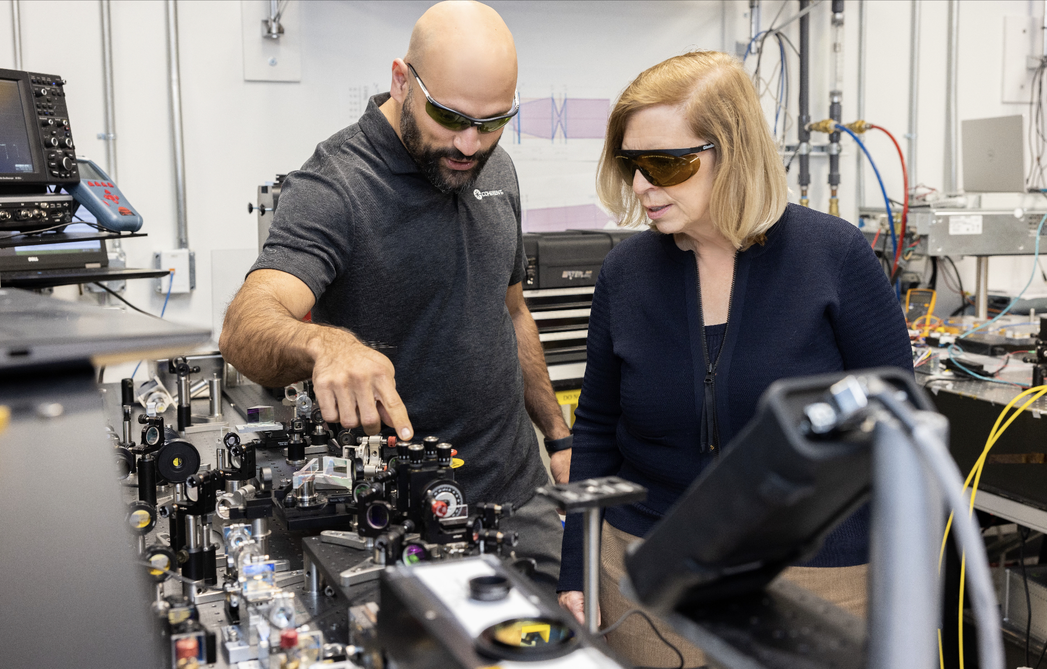
- Eng is four months into her new role as CTO of Coherent.
- Previously, she headed Finisar’s transceiver business and then the 3D sensing business, first at Finisar and then at II-VI. II-VI changed its name to Coherent in September 2022
- “CTO is one of these roles that has no universal definition,” says Eng
ulie Eng loved her previous role.
She had been heading II-VI’s (now Coherent’s) 3D sensing unit after being VP of engineering at Finisar’s transceiver business. II-VI bought Finisar in 2019.
She moved across to a new 3D sensing business while still at Finisar. The 3D sensing unit was like a start-up within a large company, she says.
II-VI and Finisar had been competitors in the 3D sensing market. Eng headed the combined units after Finisar’s acquisition.
She enjoyed the role and wasn’t looking to change when the CEO asked her to become Coherent’s CTO.
“To become CTO of the new Coherent – to help define the future of this company which is a five-plus going on six billion dollar company – that is pretty exciting,” says Eng.
The “New” Coherent
Coherent combines a broad portfolio of technologies from II-VI, Finisar, and the firm Coherent which II-VI acquired in 2022.
Just within lasers, Coherent’s portfolio spans from devices 1mm wide that are sold into mobile phones to the former Coherent’s lasers that are meters wide and used for OLED manufacturing.
Being CTO is different from Eng’s line-management roles, which had set, tangible annual goals.
Her role now is to shepherd the company’s technologies and grow the business over the long term.
Eng has been familiarising herself with the company’s technologies. To this aim, Eng is drawing on deep technological expertise across the company’s units.
Luckily, lasers are already covered, she quips.
“One of the things that I always somehow had a knack for is interacting with customers, sensing opportunities, and then figuring out how our technologies can help customers solve their problems,” says Eng.
It is a skill she successfully transferred to the consumer – 3D sensing – business but now it will be needed on a broader scale.
Eng is also making connections across technology units within the company as she seeks to identify new technologies and new market opportunities.
Her CTO role also allows her to engage with every Coherent customer across the company’s many markets.
She admits being CTO is challenging. One issue is grappling with the breadth of technologies the company has. Another is how to assess her works’ impact.
She and the CEO have discussed how best to use her time to benefit the company. Eng has also talked to other companies’ CTOs about the role and what works for them.
“It’s very interesting; CTO is one of these roles that has no universal definition,” says Eng.
Technologies to watch
Eng highlights several developments when asked about noteworthy technologies.
For communications, this is the year when 200 gigabits per lane will likely be achieved.
“The first transceivers I worked on were [SONET/SDH] OC-3 which is 155 megabits per second (Mbps),” she says. “Is wasn’t even a transceiver back then; it was discrete transmitters and receivers.”
That the industry has accelerated technology to achieve multiple lanes of 200 gigabit-per-second (Gbps) in a pluggable module is remarkable, she says.
Eng also notes Coherent’s work on a continuous-wave laser integrated with a Mach-Zehnder modulator – a DMZ – to enable 200 gigabits per lane.
The company is also active in life sciences and health monitoring. Communications, especially during the pandemic, showed its importance in people’s lives. “But life sciences and health-related products have a much more direct impact on people,” says Eng. “That is not something I’ve had direct exposure to.”
Life sciences and health monitoring is a segment where optics and optical devices will play a growing role over time.
Medical devices often originate in research environments such as hospital labs before becoming medical instruments. From the lab, they go to clinical. “What we are talking about here is going from lab to clinical to therapeutics,” she says.
The US Chips Act also heartens Eng: “It was about time for the US to prioritise semiconductors.”
Low-power coherent DSPs
Coherent and ADVA jointly developed a low-power coherent digital signal processor (DSP) and optics design for a 100-gigabit ZR (100ZR) design that fits within a QSFP28 module.
“We have an internal DSP team, and they are developing DSPs for the coherent optics market,” says Eng, adding that having the design team gives Coherent options.
Meanwhile, the debate about direct detection technology versus coherent optics continues.
As optical lane speed increases from 100 gigabits to 200 gigabits, the question remains what reach will direct detection achieve before running out of steam?
With 200 gigabits per lane, 800 gigabit modules can be achieved using four optical lanes, while for 1.6 terabits, eight lanes will be used.
Eng is confident that direct detection will support 10km at these speeds. Beyond 10km, direct detection becomes much more of a challenge, and coherent is an option.
“The real question is will coherent optics meet the size, cost and power consumption expectations of the data centre customers on a timeframe that meets their needs,” says Eng.
Having in-house DSP technology means Coherent can undertake design trade-offs and make the right decisions, she says.
After 1.6 terabits, the design options include increasing the lane rate, using more than eight channels or adopting more advanced modulation schemes.
“We look at the application, the timeline that the product needs to be released, the readiness of the technology, we do measurements – simulations – and we make objective decisions based on the results,” says Eng.
Whatever the prevalent technology is, says Eng, that technology will continue to improve since that is the livelihood of many companies.
“All of us, as an industry, are going to put our all into extending the technologies we currently have,” says Eng. So, when it comes to direct detection versus coherent, everyone will push direct detect technology as far as possible.
“Getting up to 1.6 terabits [using direct detect], that is pretty good,” says Eng. “That is going to last us a pretty long time.”
Materials
Coherent’s toolbox of material systems covers indium phosphide, silicon photonics, and gallium arsenide. It also has silicon carbide, a semiconductor suited for high-power transistors used for power electronics applications.
“We have all the technologies, we use the best technology for the product, and we use good engineering judgement,” says Eng.
Rather than favour indium phosphide or silicon photonics, Eng’s segmentation starts with whether the design is directly modulated or externally modulated.
Until now, up to 50 gigabits per lane has been well served by directly modulated lasers. This has used indium phosphide or, in the case of VCSELs, gallium arsenide.
“In general, directly modulated is the lower cost because the die is tiny, and often it is the lowest power,” says Eng.
But increasing the speed beyond 50Gbps gets more complicated with directly modulated lasers. This is where externally modulated lasers come in.
“Once you are already talking about an externally modulated solution, we start looking at the trade-offs between indium phosphide and silicon photonics,” says Eng.
The laser remains indium phosphide, so the bake-off concerns the modulator and the passive optics.
What indium phosphide brings is better electro-optics performance, while silicon photonics brings the benefits of integration.
“So if there is a high-lane count – lots of passives – or an opportunity to use one laser over multiple modulators, these can be complicated designs, and silicon photonics can help reduce the size,” says Eng.

Pluggables and co-packaged optics
With 200 gigabits per lane becoming available, there is a clear roadmap for 800-gigabits and 1.6-terabit pluggables.
“Customers like pluggables, and I don’t think people should underestimate that,” says Eng, adding that continued innovation will extend their lifetime.
“There are flyover cables between the switch ASIC and the modules, vertical line cards have been proposed, and we have shown board-mounted optical assemblies,” she says.
At some point, co-packaged optics may be the right solution, says Eng. But that will depend on the application’s specification, issues such as bandwidth, size, cost, power consumption and reliability.
“People will only transition to optical input-output when extending pluggables doesn’t make sense anymore,” says Eng. “I think it is probably five-plus years away, but there are probably error bars on that.”
Coherent’s activities include using indium phosphide manufacturing for external laser sources for co-package optics. “And we are working on silicon photonics,” she says.
Coherent is also working on co-packaging VCSELs with high-performance chips. “Not all applications require a 2km reach,” she says.

The coming decade’s opportunities
Eng’s thoughts about the growth opportunities for the coming decade are, not surprisingly, viewed through Coherent’s markets focus.
She highlights four segments: communications, industrial, instrumentation, and electronics.
Fibre-optics communications will continue to grow with bandwidth. The opportunities for innovation include datacom and coherent optics.
She also notes growing interest in free-space optics and satellite communications.
“I see money being spent on that and maybe that is a place where someone like ourselves, with a lot of optics as well as bigger lasers, can play a role,” says Eng.
Precision manufacturing uses lasers in the industrial segment. Eng cites cutting, welding and marking as examples.
“We have elements used for battery manufacturing which is increasing due to electric cars,” she says.
Excimer lasers are also used for OLED and microLED display manufacturing.
“We even have optics in extreme UV steppers [used for advanced process node chip manufacturing],” she says.
For instrumentation, much of the growth is around health life sciences. Coherent makes optics that are used inside PCR testers for COVID-19. It also has engineers working on solid state lasers used for flow cytometry (the sorting of cells). She also cites gene sequencing equipment and medical imaging.
Coherent’s electronics segment refers to the consumer market. Growth here for optics and lasers include AR/VR goggles and the metaverse, wearable health monitoring, and automotive.
For automotive, lasers are used for lidar and in-cabin sensing, such as driver and passenger monitoring.
Silicon carbide is also a growth market, and its uses include the wireless market and power devices for electric vehicles.
“I like the communications market, which we see as growing, but for us, with such a broad portfolio, there are many of these other markets and products that I see as exciting for the remainder of this decade,” says Eng.

Microchip expands the choice of 1.6-terabit Ethernet PHYs
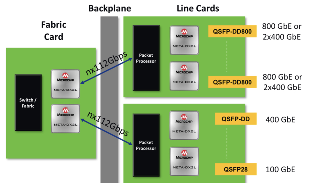
Microchip Technology has enlarged its portfolio of 1.6-terabit physical layer (PHY) Ethernet chips targeting next-generation switch and router line cards.
In 2021, Microchip announced its PM6200 Meta-DX2L (‘L’ standing for light), its first 1.6-terabit Meta-DX2 PHY that uses 112-gigabit PAM-4 (4-level pulse-amplitude modulation) serialiser/ deserialisers (series).
Microchip has now added four more 1.6-terabit Ethernet PHYs dubbed Meta-DX2+.
Like the Meta-DX2L, the PHYs are implemented using a 6nm CMOS process while the ‘plus’ signifies added features.
The Meta-DX2L is used for such tasks as retiming, for a signal sent across the system’s backplane, for example, and has a ‘gearbox’ feature that translates between 28, 56 and 112-gigabit data rates.
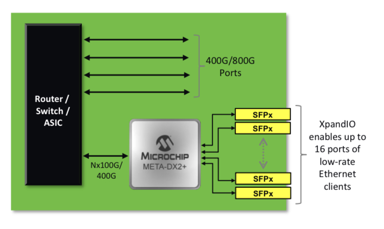
With the Meta-DX2+ PHYs, Microchip has added port aggregation and security hardware.

Security and flexibility
Microchip stresses the compact nature of its 1.6-terabit PHYs.
”We see that [compactness] as very important to our customers as they seek to double capacity and design dense systems,” says Stephen Docking, senior manager of product marketing, communications business unit at Microchip.
Security is important for cloud and enterprise, and Microchip claims it has the first PHYs supporting 1.6-terabit of capacity with MACsec and IPsec.
MACsec is used to secure traffic between distributed data centre buildings across a campus or a metropolitan region. IPsec is used for enterprise-wide area networks (WANs) where traffic goes through nodes, some of which may not support encryption.
“The intention is that we can offload those encryption engines having to be in a packet processor or switch device in a system,” says Docking.
The Meta-DX2 1.6-terabit PHYs can interface with 400-gigabit client-side pluggables, emerging 800 gigabit QSFP-DD800s, and upcoming 1.6-terabit OSFP-XD optical modules.
The 1.6 terabit PHYs effectively have two 800-gigabit cores that support rates from 1 to 800 Gigabit Ethernet.
One-gigabit Ethernet is supported as it is still used by enterprises, while 800-gigabit is soon to be deployed, says Docking.
Enterprises also require new switch devices so the 112-gigabit serdes is necessary, but many sub-100 gigabit rates remain in use. Microchip has added its XpandIO feature that aggregates low-speed ports – 1GbE, 10GbE, 25GbE, 50GbE – into the 112-gigabit PAM-4 lane to improve system efficiency.
New packet processor designs have 112-gigabit serdes. If lower rate speeds are fed directly to the packet processor, bandwidth is wasted. Microchip’s XpandIO feature aggregates these lower rates to better match the packet processor’s serdes speed.
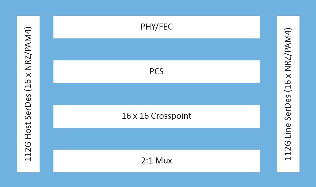
The Meta-DX2+ PHY, like the Meta-DX2L, also feature a hitless 2:1 multiplexer. The multiplexer function is suited for central architecture switch platforms where the system intelligence resides on a central card. In contrast, the connecting line cards are relatively simple, comprising PHYs and optical modules.
In such systems, because of the central role of the platform’s switch card, a standby card is included. If the primary card fails, the backup card kicks in, whereby all the switch’s line cards connect to the backup. The 2:1 multiplexer feature in the PHY means each line card is interfaced with both switch cards: the primary and the backup.
The Meta-DX2 PHY family
The Meta-DX2 PHYs are split into two groupings, the PHYs in each group are hardware compatible such that one line card design is needed.
One group has three PHYs: the PM6200 (the Meta-DX2L), the PM6216 (the Meta-DX2+ PHY with encryption engines), and the PM6210 (a Meta-DX2+ with encryption and XpandIO). All three measure 23x30mm.
The two other Meta-DX2+ PHYs – the PM6214 and the PM6218 (with encryption) – are larger ICs, 33x33mm. This is because the PHYs have 48, 100-gigabit serdes instead of 32 serdes of the first group.
The extra 16 100-gigabit serdes enable the PHYs to support, for example, 16 100-gigabit lanes (1.6-terabit) when connected to a switch IC as well as 32 lanes of 50-gigabit serdes used in 8×50-gigabit 400-gigabit QSFP-DD modules.
“The PHY package size, in this case, is larger,” says Docking. “But even with that, we still have a net 20 per cent reduction in total area.” That can make a difference between fitting in a one rack unit (1RU) design rather than 2RU.
All PHYs share a common software development kit. The software kit also supports the switch abstraction interface standard. “This decouples the operating systems from the underlying hardware,” says Dorking.
The Meta-DX2+ PHYs have been sampling since the final quarter of 2022 and the chips are available for prototypes.
Applications
The PHY portfolio caters for several classes of system designs. Microchip cites cloud and enterprise data centre switches and routers, service provider routers, encryption boxes, and optical transport platforms.

Microchip says that the Meta-DX2L was released to address the first generation of higher capacity line cards where retiming and gearbox rate changes are essential.
The remaining 1.6-terabit PHYs available now better address system vendors’ second-generation card designs that typically add features such as encryption.
What next?

A next obvious PHY family will be when the 224-gigabit electrical interface becomes available.
Microchip says it has invested more in this generation of 112-gigabit series-based PHYs than previous generations and it expects 112-gigabit serdes to be more of a ‘workhorse’ than in the past.
“I think what you will find is more 112-gigabit based solutions rather than every new investment cycle being a new line rate,” says Kevin So, director, product line management and marketing, communications business unit at Microchip.
It will not be the cadence of investments that changes, rather those investments will likely be anchored around the 112-gigabit electrical interface.
Microchip’s compact, low-power 1.6-terabit PHY

Microchip Technology’s latest physical layer (PHY) chip has been developed for next-generation line cards.
The PM6200 Meta-DX2L (the ‘L’ is for light) 1.6-terabit chip is implemented using TSMC’s 6nm CMOS process. It is Microchip’s first PHY to use 112-gigabit PAM-4 (4-level pulse-amplitude modulation) serialiser/ deserialisers (serdes) interfaces.
Microchip’s existing 16nm CMOS Meta-DX1 PHY devices are rated at 1.2 terabits and use 56-gigabit PAM-4 serdes.
System vendors developing line cards that double the capacity of their switch, router or transport systems are being challenged by space and power constraints, says Microchip. To this aim, the company has streamlined the Meta-DX2L to create a compact, lower-power chip.
“One of the things we have focussed on is the overall footprint of our [IC] design to ensure that people can realise their cards as they go to the 112-gigabit PAM-4 generation,” says Stephen Docking, manager, product marketing, communications business unit, at Microchip.
The company says the resulting package measures 23x30mm and reduces the power per port by 35 per cent compared to the Meta-DX1.
IC architecture
The Meta-DX1 family of 1.2-terabit physical layer (PHY) Ethernet chips effectively comprise three 400-gigabit cores and support the OIF’s Flexible Ethernet (FlexE) protocol and MACsec encryption.
The Meta-DX1 devices, launched in 2019, support the Precision Time Protocol (PTP) used to synchronise clocks across a network with high accuracy that is a requirement for 5G.
The new Meta-DX2L is a single chip although Microchip hints that other family devices will follow.
The Meta-DX2L can be viewed as comprising two 800-gigabit cores. The chip does away with FlexE and the PTP protocol but includes retiming and gearbox modes. The gearbox is used to translate between 28, 56 and 112-gigabit rates.
“We still see customers working on FlexE designs, so the lack of it [with the Meta-DX2L] is not due to limited market demand but how we chose to optimise the chip,” says Docking.
The same applies to PTP. The Meta-DX1 performs time stamping that meets 5G’s Class C and Class D front-haul clocking requirements. “The difference with the Meta-DX2L is that it is not doing time stamping,” says Docking. But it can work with devices doing the time stamping.
“In a 5G system, if you add a PHY, you need to do it in such a way that it doesn’t add any uncertainty in the overall latency of the system,” says Docking. ”So we have focussed on the device have a constant latency.” This means the Meta-DX2L can be used in systems meeting Class C or Class D clocking requirements.
The chip also features a 16×16 crosspoint switch that allows customers to use different types of optical modules and interface them to a line card’s ASIC or digital signal processor (DSP).
The Meta-DX2L’s two cores are flexible and support rates from 1 to 800 Gigabit Ethernet, says Docking.
As well as Ethernet rates, the device supports proprietary rates common with artificial intelligence (AI) and machine learning.
For AI, an array of graphic processor units (GPUs) talk to each other on the same line card. “But to scale the system, you have to have multiple line cards talk to each other,” says Docking. “Different companies that design GPUs have chosen their own protocols to optimise their communications.”
Such links are not aligned with the Ethernet rates but the Meta-DX2L supports these proprietary rates.
Microchip says the Meta-DX2L will sample this quarter.
1.6 terabits, system resilience and design challenges
The PHY’s 1.6-terabit capacity was chosen based on customers’ requirements.
“If you look at the number of ports people want to support, it is often an even multiple of 800-gigabit ports,” says Docking.
The Meta-DX2L, like its predecessor PHY family, has a hitless 2:1 multiplexer. The multiplexer function is suited for centralised switch platforms where the system intelligence resides on a central card while the connecting line cards are relatively simple, typically comprising PHYs and optical modules.
In such systems, due to the central role of the platform’s switch card, a spare card is included. Should the primary card fail, the backup card kicks in, whereby all the switch’s line cards connect to the backup. The 2:1 multiplexer in the PHY means each line card is interfaced to both switch cards: the primary one and backup.

For line cards that will have 32 or 36 QSFP-DD800 pluggable modules, space is a huge challenge, says Docking: “So having a compact PHY is important.”
“The physical form factor has always been a challenge and then density plays into it and thermal issues,” says Kevin So, associate director, product line management and marketing, communications business unit, at Microchip. “And when you overlay the complexity of the transition from 56 to 112 gigabits, that makes it extremely challenging for board designers.”
Applications
The 1.6-terabit PHY is aimed at switching and routing platforms, compact data centre interconnect systems, optical transport and AI designs.
Which application takes off first depends on several developments. On one side of the PHY chip sits the optics and on the other the ASIC, whether a packet processor, switch chip, processor or DSP. “It’s the timing of those pieces that drive what applications you will see first,” says So.
“Switching and packet processor chips are transitioning to 112-gigabit serdes and you are also starting to see QSFP-DD or OSFP optics with 112-gigabit serdes becoming available,” adds Docking. “So the ecosystem is starting for those types of systems.”
The device is also being aimed at routers for 5G backhaul applications. Here data rates are in the 10- to the 100-gigabit range. “But you are already starting to hear about 400-gigabit rates for some of these access backhaul routers,” says So.
And with 400 Gigabit Ethernet being introduced on access pizza-box routers for 5G this year, in two years, when Microchip’s customers release their hardware, there will likely be denser versions, says So.
“And by then we’ll be talking about a DX3, who knows?” quips So.

COBO issues industry’s first on-board optics specification
- COBO modules supports 400-gigabit and 800-gigabit data rates
- Two electrical interfaces have been specified: 8 and 16 lanes of 50-gigabit PAM-4 signals.
- There are three module classes to support designs ranging from client-slide multi-mode to line-side coherent optics.
- COBO on-board optics will be able to support 800 gigabits and 1.6 terabits once 100-gigabit PAM-4 electrical signals are specified.
 Source: COBO
Interoperable on-board optics has moved a step closer with the publication of the industry’s first specification by the Consortium for On-Board Optics (COBO).
COBO has specified modules capable of 400-gigabits and 800-gigabits rates. The designs will also support 800-gigabit and 1.6-terabit rates with the advent of 100-gigabit single-lane electrical signals.
“Four hundred gigabits can be solved using pluggable optics,” says Brad Booth, chair of COBO and principal network architect for Microsoft’s Azure Infrastructure. “But if I have to solve 1.6 terabits in a module, there is nothing out there but COBO, and we are ready.”
Origins
COBO was established three years ago to create a common specification for optics that reside on the motherboard. On-board optics is not a new technology but until now designs have been proprietary.
I have to solve 1.6 terabits in a module, there is nothing out there but COBO, and we are ready
 Brad BoothSuch optics are needed to help address platform design challenges caused by continual traffic growth.
Getting data on and off switch chips that are doubling in capacity every two to three years is one such challenge. The input-output (I/O) circuitry of such chips consumes significant power and takes up valuable chip area.
There are also systems challenges such as routing the high-speed signals from the chip to the pluggable optics on the platform’s faceplate. The pluggable modules also occupy much of the faceplate area and that impedes the air flow needed to cool the platform.
Using optics on the motherboard next to the chip instead of pluggables reduces the power consumed by shortening the electrical traces linking the two. Fibre rather than electrical signals then carries the data to the faceplate, benefiting signal integrity and freeing faceplate area for the cooling.
Specification 1.0
COBO has specified two high-speed electrical interfaces. One is 8-lanes wide, each lane being a 50-gigabit 4-level pulse-amplitude modulation (PAM-4) signal. The interface is based on the IEEE’s 400GAUI-8, the eight-lane electrical specification developed for 400 Gigabit Ethernet.
The second electrical interface is a 16-lane version for an 800-gigabit module. Using a 16-lane design reduces packaging costs by creating an 800-gigabit module instead using two separate 400-gigabit ones. Heat management is also simpler with one module.
There are also systems benefits using an 800-gigabit module.“As we go to higher and higher switch silicon bandwidths, I don’t have to populate as many modules on the motherboard,” says Booth.
The latest switch chips announced by several companies have 12.8 terabits of capacity that will require 32, 400-gigabit on-board modules but only 16, 800-gigabit ones. Fewer modules simplify the board’s wiring and the fibre cabling to the faceplate.
Designers have a choice of optical formats using the wider-lane module, such as 8x100 gigabits, 2x400 gigabits, and even 800 gigabits.
COBO has tested its design and shown it can support a 100-gigabit electrical interface. The design uses the same connector as the OSFP pluggable module.
“In essence, with an 8-lane width, we could support an 800-gigabit module if that is what the IEEE decides to do next,” says Booth. “We could also support 1.6 terabits if that is the next speed hop.”
It is very hard to move people from their standard operating model to something else until there is an extreme pain point
Form factor and module classes
The approach chosen by COBO differs from proprietary on-board optics designs in that the optics is not mounted directly onto the board. Instead, the COBO module resembles a pluggable in that once placed onto the board, it slides horizontally to connect to the electrical interface (see diagram, top).
A second connector in the middle of the COBO module houses the power, ground and control signals. Separating these signals from the high-speed interface reduces the noise on the data signals. In turn, the two connectors act as pillars supporting the module.
The robust design allows the modules to be mounted at the factory such that the platform is ready for operation once delivered at a site, says Booth.
COBO has defined three module classes that differ in length. The shortest Class A modules are used for 400-gigabit multi-mode interfaces while Class B suits higher-power IEEE interfaces such as 400GBASE-DR4 and the 100G Lambda MSA’s 400G-FR4.
The largest Class C module is for the most demanding and power-hungry designs such as the coherent 400ZR standard. “Class C will be able to handle all the necessary components - the optics and the DSP - associated with that [coherent design],” says Booth.
The advantage of the on-board optics is that it is not confined to a cage as pluggables are. “With an on-board optical module, you can control the heat dissipation by the height of the heat sink,” says Booth. “The modules sit flatter to the board and we can put larger heat sinks onto these devices.”
We realised we needed something as a stepping stone [between pluggables and co-packaged optics] and that is where COBO sits
Next steps
COBO will develop compliance-testing boards so that companies developing COBO modules can verify their designs. Booth hopes that by the ECOC 2018 show to be held in September, companies will be able to demonstrate COBO-based switches and even modules.
COBO will also embrace 100-gigabit electrical work being undertaken by the OIF and the IEEE to determine what needs to be done to support 8-lane and 16-lane designs. For example, whether the forward-error correction needs to be modified or whether existing codes are sufficient.
Booth admits that the industry remains rooted to using pluggables, while the move to co-packaged optics, where the optics and the chip are combined in the same module - remains a significant hurdle, both in terms of packaging technology and the need for vendors to change their business models to build such designs.
“It is very hard to move people from their standard operating model to something else until there is an extreme pain point,” says Booth.
Setting up COBO followed the realisation that a point would be reached when faceplate pluggables would no longer meet demands while in-packaged technology would not be ready.
“We realised we needed something as a stepping stone and that is where COBO sits,” says Booth.
Further information
For information on the COBO specification, click here.