
Optical integration and silicon photonics: A view to 2021
LightCounting’s report on photonic integration has several notable findings. The first is that only one in 40 optical components sold in the datacom and telecom markets is an integrated device yet such components account for a third of total revenues.

Another finding is that silicon photonics will not have a significant market impact in the next five years to 2021, although its size will grow threefold in that time.
By 2021, one in 10 optical components will be integrated and will account for 40% of the total market, while silicon photonics will become a $1 billion industry by then.
Integrated optics
“Contrary to the expectation that integration is helping to reduce the cost of components, it is only being used for very high-end products,” says Vladimir Kozlov, CEO of LightCounting.
He cites the example of the cost-conscious fibre-to-the-home market which despite boasting 100 million units in 2015 - the highest volumes in any one market - uses discrete parts for its transceivers. “There is very little need for optical integration in this high-volume, low-cost market,” he says
Where integration is finding success is where it benefits device functionality. “Where it takes the scale of components to the next level, meaning much more sophisticated designs than just co-packaged discrete parts,” says Kozlov. And it is because optical integration is being applied to high-end, costlier components that explains why revenues are high despite volumes being only 2.4% of the total market.
Defining integration
LightCounting is liberal in its definition of an integrated component. An electro-absorption modulated laser (EML) where the laser and modulator are on the same chip is considered as an integrated device. “It was developed 20 years ago but is just reaching prime time now with line rates going to 25 gigabit,” says Kozlov.
Designs that integrate multiple laser chips into a transceiver such as a 4x10 gigabit design is also considered an integrated design. “There is some level of integration; it is more sophisticated than four TO-cans,” says Kozlov. “But you could argue it is borderline co-packaging.”
LightCounting forecasts that integrated products will continue to be used for high-end designs in the coming five years. This runs counter to the theory of technological disruption where new technologies are embraced at the low end first before going on to dominate a market.
“We see it continuing to enter the market for high-end products simply because there is no need for integration for very simple optical parts,” says Kozlov.
Silicon photonics
LightCounting does not view silicon photonics as a disruptive technology but Kozlov acknowledges that while the technology has performance disadvantages compared to traditional technologies such as indium phosphide and gallium arsenide, its optical performance is continually improving. “That may still be consistent with the theory of technological disruption,” he says.
There are all these concerns about challenges but silicon photonics does have a chance to be really great
The market is also developing in a way that plays to silicon photonics’ strengths. One such development is the need for higher-speed interfaces, driven by large-scale data centre players such as Microsoft. “Their appetite increases as the industry is making progress,” says Kozlov. “Six months ago they were happy with 100 gigabit, now they are really focused on 400 gigabit.”
Going to 400 gigabit interfaces will need 4-level pulse-amplitude modulation (PAM4) transmitters that will provide new ground for competition between indium phosphide, VCSELs and silicon photonics, says Kozlov. Silicon photonics may even have an edge according to results from Cisco where its silicon photonics-based modulators were shown to work well with PAM4. This is where silicon photonics could even take a market lead: for 400-gigabit designs that require multiple PAM4 transmitters on a chip, says LightCounting.
Another promise silicon photonics could deliver although yet to be demonstrated is the combination of optics and electronics in one package. Such next-generation 3D packaging, if successful, could change things more dramatically than LightCounting currently anticipates, says Kozlov.
“This is the interesting thing about technology, you never really know how successful it will be,” says Kozlov. “There are all these concerns about challenges but silicon photonics does have a chance to be really great.”
But while LightCounting is confident the technology will prove successful sooner of later, getting businesses that use the technology to thrive will require overcoming a completely different set of challenges.
“It is a challenging environment,” warns Kozlov. “There is probably more risk on the business side of things now than on the technology side.”
Tackling system design on a data centre scale
Interview 1: Andrew Rickman
Silicon photonics has been a recurring theme in the career of Andrew Rickman. First, as a researcher looking at the feasibility of silicon-based optical waveguides, then as founder of Bookham Technologies, and after that as a board member of silicon photonics start-up, Kotura.
 Andrew Rickman
Now as CEO of start-up Rockley Photonics, his company is using silicon photonics alongside its custom ASIC and software to tackle a core problem in the data centre: how to connect more and more servers in a cost effective and scaleable way.
Origins
As a child, Rickman attended the Royal Institution Christmas Lectures given by Eric Laithwaite, a popular scientist who was also a professor of electrical engineering at Imperial College. As an undergraduate at Imperial, Rickman was reacquainted with Professor Laithwaite who kindled his interest in gyroscopes.
“I stumbled across a device called a fibre-optic gyroscope,” says Rickman. “Within that I could see people starting to use lithium niobate photonic circuits.” It was investigating the gyroscope design and how clever it was that made Rickman wonder whether the optical circuits of such a device could be made using silicon rather than exotic materials like lithium niobate.
“That is where the idea triggered, to look at the possibility of being able to make optical circuits in silicon,” he says.
If you try and force a photon into a space shorter than its wavelength, it behaves very badly
In the 1980s, few people had thought about silicon in such a context. That may seem strange today, he says, but silicon was not a promising candidate material. “It is not a direct band-gap material - it was not offering up the light source, and it did not have a big electro-optic effect like lithium niobate which was good for modulators,” he says. “And no one had demonstrated a low-loss single-mode waveguide.”
Rickman worked as a researcher at the University of Surrey’s physics department with such colleagues as Graham Reed to investigate whether the trillions of dollars invested in the manufacturing of silicon could also be used to benefit photonic circuits and in particular whether silicon could be used to make waveguides. “The fundamental thing one needed was a viable waveguide,” he says.
Rickman even wrote a paper with Richard Soref who was collaborating with the University of Surrey at the time. “Everyone would agree that Richard Soref is the founding father of the idea - the proposal of having a useful waveguide in silicon - which is the starting point,” says Rickman. It was the work at the University of Surrey, sponsored by Bookham which Rickman had by then founded, that demonstrated low-loss waveguides in silicon.
Fabrication challenges
Rickman argues that not having a background in CMOS processes has been a benefit. “I wasn’t dyed-in-the-wool-committed to CMOS-type electronics processing,” he says. “I looked upon silicon technology as a set of machine-shop processes for making things.”
Looking at CMOS processing completely afresh and designing circuits optimised for photonics yielded Bookham a great number of high-performance products, he says. In contrast, the industry’s thrust has been very much a semiconductor CMOS-focused one. “People became interested in photonics because they just naturally thought it was going to be important in silicon, to perpetuate Moore’s law,” says Rickman.
You can use the structures and much of the CMOS processes to make optical waveguides, he says, but the problem is you create small structures - sub-micron - that guide light poorly. “If you try and force a photon into a space shorter than its wavelength, it behaves very badly,” he says. “In microelectronics, an electron has got a wavelength that is one hundred times smaller that the features it is using.”
The results include light being sensitive to interface roughness and to the manufacturing tolerances - the width, hight and composition of the waveguide. “At least an order of magnitude more difficult to control that the best processes that exist,” says Rickman.
“Our [Rockley’s] waveguides are one thousand times more relaxed to produce than the competitors’ smaller ones,” he says. “From a process point of view, we don’t need the latest CMOS node, we are more a MEMS process.”
If you take control of enough of the system problem, and you are not dictated to in terms of what MSA or what standard that component must fit into, and you are not competing in this brutal transceiver market, then that is when you can optimise the utilisation of silicon photonics
Rickman stresses that small waveguides do have merits - they go round tighter bends, and their smaller-dimensioned junctions make for higher-speed components. But using very large features solves the ‘fibre connectivity problem’, and Rockley has come up with its own solutions to achieve higher-speed devices and dense designs.
“Bookham was very strong in passive optics and micro-engineered features,” says Rickman. “We have taken that experience and designed a process that has all the advantages of a smaller process - speed and compactness - as well as all the benefits of a larger technology: the multiplexing and demultiplexing for doing dense WDM, and we can make a chip that already has a connector on it.”
Playing to silicon photonics’ strengths
Rickman believes that silicon photonics is a significant technological development: “It is a paradigm shift; it is not a linear improvement”. But what is key is how silicon photonics is applied and the problem it is addressing.
To make an optical component for an interface standard or a transceiver MSA using silicon photonics, or to use it as an add-on to semiconductors - a ’band-aid” – to prolong Moore’s law, is to undersell its full potential. Instead, he recommends using silicon photonics as one element - albeit an important one - in an array of technologies to tackle system-scale issues.
“If you take control of enough of the system problem, and you are not dictated to in terms of what MSA or what standard that component must fit into, and you are not competing in this brutal transceiver market, then that is when you can optimise the utilisation of silicon photonics,” says Rickman. “And that is what we are doing.” In other words, taking control of the environment that the silicon sits in.
It [silicon photonics] is a paradigm shift; it is not a linear improvement
Rockley’s team has been structured with the view to tackle the system-scale problem of interconnecting servers in the data centre. Its team comprises computer scientists, CMOS designers - digital and analogue - and silicon photonics experts.
Knowing what can be done with the technologies and organising them allows the problems caused by the ‘exhaustion of Moore’s law’ and the input/output (I/O) issues that result to be overcome. “Not how you apply one technology to make up for the problems in another technology,” says Rickman.
The ending of Moore’s law
Moore’s law continues to deliver a doubling of transistors every two years but the associated scaling benefits like the halving of power consumed per transistor no longer apply. As a result, while Moore’s law continues to grow gate count that drives greater computation, the overall power consumption is no longer constant.
Rickman also points out that the I/O - the number of connections on and off a chip - are not doubling with transistor count. “I/O may be going from 25 gigabit to 50 gigabit using PAM–4 but there are many challenges and the technology has yet to be demonstrated,” he says.
The challenge facing the industry is that increasing the I/O rate inevitably increases power consumption. “As power consumption goes up, it also equates to cost,” says Rickman. Clearly that is unwelcome and adds cost, he says, but that is not the only issue. As power goes up, you cannot fully benefit from the doubling transistor counts, so things cannot be packed more densely.
“You are running into to the end of Moore’s law and you don’t get the benefit of reducing space and cost because you’ve got to bolt on all these other things as it is very difficult to get all these signals off-chip,” he says.
This is where tackling the system as a whole comes in. You can look at microelectronics in isolation and use silicon photonics for chip-to-chip communications across a printed circuit board to reduce the electrical losses through the copper traces. “A good thing to do,” stresses Rickman. Or you can address, as Rockley aims to do, Moore’s law and the I/O limitations within a complete system the size of the data centre that links hundred of thousands of computers. “Not the same way you’d solve an individual problem in an individual device,” says Rickman.
Rockley Photonics
Rockley Photonics has already demonstrated all the basic elements of its design. “That has gone very well,” says Rickman.
The start-up has stated its switch design uses silicon photonics for optical switching and that the company is developing an accompanying controller ASIC. It has also developed a switching protocol to run on the hardware. Rockley’s silicon photonics design performs multiplexing and demultiplexing, suggesting that dense WDM is being used as well as optical switching.
Rockley is a fabless semiconductor company and will not be building systems. Partly, it is because it is addressing the data centre and the market has evolved in a different way to telecoms. For the data centre, there are established switch vendors and white-box manufacturers. As such, Rockley will provide its chipset-based reference design, its architecture IP and the software stack for its customers. “Then, working with the customer contract manufacturer, we will implement the line cards and the fabric cards in the format that the particular customer wants,” says Rickman.
The resulting system is designed as a drop-in replacement for the large-scale data centre players’ switches they haver already deployed, yet will be cheaper, more compact and consume less power, says Rockley.
“They [the data centre operators] can scale the way they do at the moment, or they can scale with our topology,” says Rickman.
The start-up expects to finally unveil its technology by the year end.
OFC 2016: a sample of the technical paper highlights
Here is a small sample of the technical paper highlights being presented at the conference.
Doubling core network capacity
Microsoft has conducted a study measuring the performance of its North American core backbone network to determine how the use of bandwidth-variable transceivers (BVTs) could boost capacity.
The highest capacity modulation scheme suited for each link from the choice of polarisation-multiplexed, quadrature phase-shift keying (PM-QPSK), polarisation-multiplexed, 8 quadrature amplitude modulation (PM-8QAM) and PM-16QAM can then be used.
By measuring the signal (Q-factor) for all its PM-QPSK based 100 gigabit links, Microsoft's study found that network capacity could be increased by 70 percent using BVTs. Equally, having the ability to increase capacity in 25-gigabit increments would increase capacity by a further 16 percent while a finer resolution of 1-gigabit would add an extra 13 percent.
Microsoft says such tuning of links need not be done in real time but rather when a link is commissioned or undergoing maintenance.
[paper M2J.2]
Architecting a new metro
How can operators redesign their metro network to enable rapid service innovation? This is the subject of a joint paper from AT&T, the Open Networking Lab and Stanford University. The work is part of a programme dubbed CORD to redesign the central office as a data centre using commodity hardware and open software to enable the rapid scaling of services. In particular, OpenFlow-enabled white boxes, the Open Network Operating System (ONOS) - a software-defined networking (SDN) operating system, and network control and management applications are used.
As part of CORD, three legacy telecom devices - optical line termination (OLT), customer premises equipment (CPE), and broadband network gateways (BNG) - have been virtualised and implemented on servers.
The paper details how a single SDN control plane based on ONOS is used to create a converged packet-optical metro network and how its support for bandwidth on-demand and automatic restoration at the optical level is used for enterprise connectivity and video distribution services.
The paper also discusses how the metro architecture supports 'disaggregated' reconfigurable optical add/ drop multiplexers (ROADMs). By disaggregating a chassis-based ROADM into commodity components, an operator can size its infrastructure as required and grow it with demand, the paper says.
[paper Th1A.7]
400 gigabit single-carrier transmission
Nokia Bell Labs reports work on 400 gigabit-per-second (Gbps) single-carrier optical transmission over submarine distances. The attraction of adopting 400 gigabit single-carrier transmission as that it is the most efficient way to reduce the cost-per-bit of optical transmission systems.
The Bell Labs' paper reviews state-of-the-art 400 gigabit single-channel transmissions over 6,000km and greater distances, and discusses the tradeoffs between such variables as symbol rate, modulation and forward error correction (FEC) schemes.
400Gbps single-carrier submarine transmission is likely in the next few years
PM-16QAM is proposed as a promising modulation scheme to achieve beyond 6,000km distances and a spectral efficiency exceeding 5b/s/Hz. But this requires a symbol rate of greater than 60 gigabaud to accommodate the 20 percent overhead FEC. Pulse-shaping at the transmitter is also used.
Exploring the receiver performance with the varying symbol rate/ FEC overhead, Bell Labs reports that the best tradeoff between coding gain and implementation penalties is 64 gigabaud and 27.3% overhead. It concludes that single-carrier 400Gbps submarine transmission is likely in the next few years.
[paper Th1B.4]
Silicon modulator for CFP2-ACOs
Cisco has developed a compact flip-chip assembly that combines a silicon photonics modulator and a silicon germanium BiCMOS Mach-Zehnder modulator driver. Such an assembly forms the basis for low-cost advanced coherent optical transceivers such as the CFP2-ACO.
Cisco has demonstrated the assembly operating at 128.7Gbps using PM-QPSK and 257.3Gbps using PM-16QAM. Cisco believes this is the first demonstration of transmission at 257.3Gbps using PM-16QAM over 1,200km of standard single-mode fibre using a silicon photonics-based device.
The modulator has also been demonstrated operating at 321.4Gbps using PM-16QAM transmission and a 20 percent FEC overhead, the highest bit rate yet achieved using a silicon-photonics based transmitter, claims Cisco.
Cisco is already using CFP2-ACO modules as part of its NCS 1002 data centre interconnect platform that implement PM-16QAM and deliver 250 gigabit due to the use of a higher baud rate than the 32 gigabaud used for existing 100-gigabit coherent systems.
[paper Th1F.2]
Flexible Ethernet to exploit line-side efficiencies
Given how the optical network network is starting to use adaptive-rate interfaces, a paper from Google asks how the client side can benefit from such line-side flexibility.
The paper points out that traditional DWDM transport equipment typically multiplexes lower-rate client ports but that this doesn't apply to network operators that manage their own data centres. Here, traffic is exclusively packet-based from IP routers and typically matches the line rate. This is why data centre interconnect platforms have become popular as they require limited grooming capability.
Google highlights how Flexible Ethernet (FlexE), for which the Optical Internetworking Forum has just defined an Implementation Agreement for, combined with data centre interconnect equipment is an extremely effective combination.
FlexE supports Ethernet MAC rates independent of the Ethernet physical layer rate being used. Google shows examples of how using FlexE, sub client rates can match the line-side rate as well as how multiple client ports can support a higher speed router logical port.
The paper concludes that combining FlexE with data centre interconnect results in a low cost, low power, compact design that will enable Internet content providers to scale their networks.
[paper W4G.4]
Silicon photonics adds off-chip comms to a RISC-V processor
"For the first time a system - a microprocessor - has been able to communicate with the external world using something other than electronics," says Vladimir Stojanovic, associate professor of electrical engineering and computer science at the University of California, Berkeley.
 Vladimir Stojanovic
The microprocessor is the result of work that started at MIT nearly a decade ago as part of a project sponsored by the US Defense Advanced Research Projects Agency (DARPA) to investigate the integration of photonics and electronics for off-chip and even intra-chip communications.
The chip features a dual-core 1.65GHz RISC-V open instruction set processor and 1 megabyte of static RAM and integrates 70 million transistors and 850 optical components.
The work is also notable in that the optical components were developed without making any changes to an IBM 45nm CMOS process used to fabricate the processor. The researchers have demonstrated two of the processors communicating optically, with the RISC core on one chip reading and writing to the memory of the second device and executing programs such as image rendering.
This CMOS process approach to silicon photonics, dubbed 'zero-change' by the researchers, differs from that of the optical industry. So far silicon photonics players have customised CMOS processes to improve the optical components' performance. Many companies also develop the silicon photonics separately, using a trailing-edge 130nm or 90nm CMOS process while implementing the driver electronics on a separate chip using more advanced CMOS. That is because photonic devices such as a Mach-Zehnder modulator are relatively large and waste expensive silicon real-estate if implemented using a leading-edge process.
IBM is one player that has developed the electronics and optics on one chip using a 90nm CMOS process. However, the company says that the electronics use feature sizes closer to 65nm to achieve electrical speeds of 25 gigabit-per-second (Gbps), and being a custom process, it will only be possible to implement 50-gigabit rates using 4-level pulse amplitude modulation (PAM-4).
We are now reaping the benefits of this very precise process which others cannot do because they are operating at larger process nodes
"Our approach is that photonics is sort of like a second-class citizen to transistors but it is still good enough," says Stojanovic. This way, photonics can be part of an advanced CMOS process.
Pursuing a zero-change process was first met with skepticism and involved significant work by the researchers to develop. "People thought that making no changes to the process would be super-restrictive and lead to very poor [optical] device performance," says Stojanovic. Indeed, the first designs produced didn't work. "We didn't understand the IBM process and the masks enough, or it [the etching] would strip off certain stuff we'd put on to block certain steps."
But the team slowly mastered the process, making simple optical devices before moving on to more complex designs. Now the team believes its building-block components such as its vertical grating couplers have leading-edge performance while its ring-resonator modulator is close to matching the optical performance of designs using custom CMOS processes.
"We are now reaping the benefits of this very precise process which others cannot do because they are operating at larger process nodes," says Stojanovic.
Silicon photonics design
The researchers use a micro ring-resonator for its modulator design. The ring-resonator is much smaller than a Mach-Zehnder design and is 10 microns in diameter. Stojanovic says the dimensions of its vertical grating couplers are 10 to 20 microns while its silicon waveguides are 0.5 microns.
Photonic components are big relative to transistors, but for the links, it is the transistors that occupy more area than the photonics. "You can pack a lot of utilisation in a very small chip area," he says.
A key challenge with a micro ring-resonator is ensuring its stability. As the name implies, modulation of light occurs when the device is in resonance but this drifts with temperature, greatly impairing its performance.
Stojanovic cites how even the bit sequence can affect the modulator's temperature. "Given the microprocessor data is uncoded, you can have random bursts of zeros," he says. "When it [the modulator] drops the light, it self-heats: if it is modulating a [binary] zero it gets heated more than letting a one go through."
The researchers have had to develop circuitry that senses the bit-sequence pattern and counteracts the ring's self-heating. But the example also illustrates the advantage of combining photonics and electronics. "If you have a lot of transistors next to the modulator, it is much easier to tune it and make it work," says Stojanovic.
 A prototype set-up of the chip-to-chip interconnect using silicon photonics. Source: Vladimir Stojanovic
Demonstration
The team used two microprocessors - one CPU talking to the memory of the second chip 4m away. Two chips were used rather than one - going off-chip before returning - to prove that the communication was indeed optical since there is also an internal electrical bus on-chip linking the CPU and memory. "We wanted to demonstrate chip-to-chip because that is where we think the biggest bang for the buck is," says Stojanovic.
In the demonstration, a single laser operating at 1,183nm feeds the two paths linking the memory and processor. Each link is 2.5Gbps for a total bandwidth of 5Gbps. However the microprocessor was clocked at one-eightieth of its 1.65GHz clock speed because only one wavelength was used to carry data. The microprocessor design can support 11 wavelengths for a total bandwidth of 55Gbit/s while the silicon photonics technology itself will support between 16 and 32 wavelengths overall.
The group is already lab-testing a new iteration of the chip that promises to run the processor at full speed. The latest chip also features improved optical functions. "It has better devices all over the place: better modulators, photo-detectors and gratings; it keeps evolving," says Stojanovic.
We can ship that kind of bandwidth [3.2 terabits] from a single chip
Ayar Labs
Ayar Labs is a start-up still in stealth mode that has been established to use the zero-change silicon photonics to make interconnect chips for platforms in the data centre.
Stojanovic says the microprocessor demonstrator is an example of a product that is two generations beyond existing pluggable modules. Ayar Labs will focus on on-board optics, what he describes as the next generation of product. On-board optics sit on a card, close to the chip. Optics integrated within the chip will eventually be needed, he says, but only once applications require greater bandwidth and denser interfaces.
"One of the nice things is that this technology is malleable; it can be put in various form factors to satisfy different connectivity applications," says Stojanovic.
What Ayar Labs aims to do is replace the QSFP pluggable modules on the face plate of a switch with one chip next to the switch silicon that can have a capacity of 3.2 terabits. "We can ship that kind of bandwidth from a single chip," says Stojanovic.
Such a chip promises cost reduction given how a large part of the cost in optical design is in the packaging. Here, packaging 32, 100 Gigabit Ethernet QSFP modules can be replaced with a single optical module using the chip. "That cost reduction is the key to enabling deeper penetration of photonics, and has been a barrier for silicon photonics [volumes] to ramp," says Stojanovic.
There is also the issue of how to couple the laser to the silicon photonics chip. Stojanovic says such high-bandwidth interface ICs require multiple lasers: "You definitely don't want hundreds of lasers flip-chipped on top [of the optical chip], you have to have a different approach".
Ayar Labs has not detailed what it is doing but Stojanovic says that its approach is more radical than simply sharing one laser across a few links, "Think about the laser as the power supply to the box, or maybe a few racks," he says.
The start-up is also exploring using standard polycrystalline silicon rather than the more specialist silicon-on-isolator wafers.
"Poly-silicon is much more lossy, so we have had to do special tricks in that process to make it less so," says Stojanovic. The result is that changes are needed to be made to the process; this will not be a zero-change process. But Stojanovic says the changes are few in number and relatively simple, and that it has already been shown to work.
Having such a process available would allow photonics to be added to transistors made using the most advanced CMOS processes - 16nm and even 7nm. "Then silicon-on-insulator becomes redundant; that is our end goal,” says Stojanovic.
Further information
Single-chip microprocessor that communicates directly using light, Nature, Volume 528, 24-31 December 2015
Start-up Sicoya targets chip-to-chip interfaces

“The trend we are seeing is the optics moving very close to the processor,” says Sven Otte, Sicoya’s CEO.
Sicoya was founded last year and raised €3.5 million ($3.9 million) towards the end of 2015. Many of the company’s dozen staff previously worked at the Technical University of Berlin. Sicoya expects to grow the company’s staff to 20 by the year end.
Otte says a general goal shared by silicon photonics developers is to combine the optics with the processor but that the industry is not there yet. “Both are different chip technologies and they are not necessarily compatible,” he says. “Instead we want the ASPIC very close to the processor or even co-packaged in a system-in-package design.”
Vertical-cavity surface-emitting lasers (VCSELs) are used for embedded optics placed alongside chips. VCSELs are inexpensive to make, says Otte, but they need to be packaged with driver chips. A VCSEL also needs to be efficiently coupled to the fibre which also requires separate lenses. ”These are hand-made transceivers with someone using a microscope to assemble,” says Otte. “But this is not scalable if you are talking about hundreds of thousands or millions of parts.”
He cites the huge numbers of Intel processors used in servers. “If you want to put an optical transceiver next to each of those processors, imagine doing that with manual assembly,” says Otte. “It just does not work; not if you want to hit the price points.”
In contrast, using silicon photonics requires two separate chips. The photonics is made using an older CMOS process with 130nm or 90nm feature sizes due to the relatively large dimensions of the optical functions, while a more advanced CMOS process is used to implement the electronics - the control loops, high-speed drivers and the amplifiers - associated with the optical transceiver. If an advanced CMOS process is used to implement both the electronics and optics on the one chip, the photonics dominates the chip area.
“If you use a sophisticated CMOS process then you pay all the money for the electronics but you are really using it for the optics,” says Otte. “This is why recently the two have been split: a sophisticated CMOS process for the electronics and a legacy, older process for the optics.”
Sicoya is adopting a single-chip approach, using a 130nm silicon germanium BiCMOS process technology for the electronics and photonics, due to its tiny silicon photonics modulator. “Really it is an electronics chip with a little bit of optics,” says Otte.
You can’t make a data centre ten times larger, and data centres can’t become ten times more expensive. You need to do something new.
Modulation
The start-up does not use a traditional Mach-Zehnder modulator or the much smaller ring-resonator modulator. The basic concept of the ring resonator is that by varying the refractive index of the ring waveguide, it can build up a large intensity of light, starving light in an adjacent coupled waveguide. This blocking and passing of light is what is needed for modulation.
The size of the ring resonator is a big plus but its operation is highly temperature dependent. “One of its issues is temperature control,” says Otte. “Each degree change impacts the resonant frequency [of the modulator].” Moreover, the smaller the ring-resonator design, the more sensitive it becomes. “You may shrink the device but then you need to add a lot more [controlling] circuitry,” he says.
Stefan Meister, Sicoya’s CTO, explains that there needs to be a diode with a ring resonator to change the refractive index to perform the modulation. The diode must be efficient otherwise, the resonance region is narrow and hence more sensitive to temperature change.
Sicoya has developed its own modulator which it refers to as a node-matched diode modulator. The modulator uses a photonic crystal; a device with a periodic structure which blocks certain frequencies of light. Sicoya’s modulator acts like a Fabry-Perot resonator and uses an inverse spectrum approach. “It has a really efficient diode inside so that the Q factor of the resonator can be really low,” says Meister. “So the issue of temperature is much more relaxed.” The Q factor refers to the narrowness of the resonance region.
Operating based on the inverse spectrum also results in Sicoya’s modulator having a much lower loss, says Meister.
Sicoya is working with the German foundry IHP to develop its technology and claims its modulator has been demonstrated operating at 25 gigabit and at 50 gigabit. But the start-up is not yet ready to detail its ASPIC designs nor when it expects to launch its first product.
5G wireless
However the CEO believes such technology will be needed with the advent of 5G wireless. The 10x increase in broadband bandwidth that the 5G cellular standard promises coupled with the continual growth of mobile subscribers globally will hugely impact data centres.
“You can’t make a data centre ten times larger, and data centres can’t become ten times more expensive, says Otte. “You need to do something new.”
This is where Sicoya believes its ASPICs can play a role.
“You can forward or process ten times the data and you are not paying more for it,” says Otte. “The transceiver chip is not really more expensive than the driver chip.”
Ciena shops for photonic technology for line-side edge
Part 3: Acquisitions and silicon photonics
Ciena is to acquire the high-speed photonics components division of Teraxion for $32 million. The deal includes 35 employees and Teraxion’s indium phosphide and silicon photonics technologies. The systems vendor is making the acquisition to benefit its coherent-based packet-optical transmission systems in metro and long-haul networks.
 Sterling Perrin
“Historically Ciena has been a step ahead of others in introducing new coherent capabilities to the market,” says Ron Kline, principal analyst, intelligent networks at market research company, Ovum. “The technology is critical to own if they want to maintain their edge.”
“Bringing in-house not everything, just piece parts, are becoming differentiators,” says Sterling Perrin, senior analyst at Heavy Reading.
Ciena designs its own WaveLogic coherent DSP-ASICs but buys its optical components. Having its own photonics design team with expertise in indium-phosphide and silicon photonics will allow Ciena to develop complete line-side systems, optimising the photonics and electronics to benefit system performance.
Owning both the photonics and optics also promises to reduce power consumption and improve line-side port density.
“These assets will give us greater control of a critical roadmap component for the advancement of those coherent solutions,” a Ciena spokesperson told Gazettabyte. “These assets will give us greater control of a critical enabling technology to accelerate the pace of our innovation and speed our time-to-market for key packet-optical solutions.”
Ciena have always been do-it-yourself when it comes to optics, and it is an area where they has a huge heritage. So it is an interesting admission that they need somebody else to help them.
The OME 6500 packet optical platform remains a critical system for Ciena in terms of revenues, according to a recent report from the financial analyst firm, Jefferies.
Ciena have always been do-it-yourself when it comes to optics, and it is an area where they have a huge heritage, says Perrin: “So it is an interesting admission that they need somebody else to help them.” It is the silicon photonics technology not just photonic integration that is of importance to Ciena, he says.
Coherent competition
Infinera, which designs its own photonic integrated circuits (PICs) and coherent DSP-ASIC, recently detailed its next-generation coherent toolkit prior to the launch of its terabit PIC and coherent DSP-ASIC. The toolkit uses sub-carriers, parallel processing soft-decision forward-error correction (SD-FEC) and enhanced modulation techniques. These improvements reflect the tighter integration between photonics and electronics for optical transport.
Cisco Systems is another system vendor that develops its own coherent ASICs and has silicon photonics expertise with its Lightwire acquisition in 2012, as does Coriant which works with strategic partners while using merchant coherent processors. Huawei has photonic integration expertise with its acquisitions of indium phosphide UK specialist CIP Technologies in 2012 and Belgian silicon photonics start-up Caliopa in 2013.
Cisco may have started the ball rolling when they acquired silicon photonics start-up Lightwire, and at the time they were criticised for doing so, says Perrin: “This [Ciena move] seems to be partially a response, at least a validation, to what Cisco did, bringing that in-house.”
Optical module maker Acacia also has silicon photonics and DSP-ASIC expertise. Acacia has launched 100 gigabit and 200-400 gigabit CFP optical modules that use silicon photonics.
Companies like Coriant and lots of mid-tier players can use Acacia and rely on the expertise the start-up is driving in photonic integration on the line side, says Perrin. ”Now Ciena wants to own the whole thing which, to me, means they need to move more rapidly, probably driven by the Acacia development.”
Teraxion
Ciena has been working with Canadian firm Teraxion for a long time and the two have a co-development agreement, says Perrin.
Teraxion was founded in 2000 during the optical boom, specialising in dispersion compensation modules and fibre Bragg gratings. In recent years, it has added indium-phosphide and silicon photonics expertise and in 2013 acquired Cogo Optronics, adding indium-phosphide modulator technology.
Teraxion detailed an indium phosphide modulator suited to 400 gigabit at ECOC 2015. Teraxion said at the time that it had demonstrated a 400-gigabit single-wavelength transmission over 500km using polarisation-multiplexed, 16-QAM (PM-16QAM), operating at a symbol rate of 56 gigabaud.
It also has a coherent receiver technology implemented using silicon photonics.
The remaining business of Teraxion covers fibre-optic communication, fibre lasers and optical-sensing applications which employs 120 staff will continue in Québec City.
MultiPhy raises $17M to develop 100G serial interfaces
MultiPhy is developing chips to support serial 100-gigabit-per-second transmission using 25-gigabit optical components. The design will enable short reach links within the data centre and up to 80km point-to-point links for data centre interconnect.
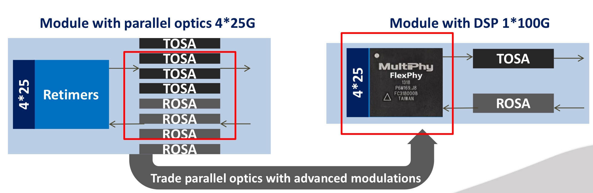 Source: MultiPhy
“It is not the same chip [for the two applications] but the same technology core,” says Avi Shabtai, the CEO of MultiPhy. The funding will be used to bring products to market as well as expand the company’s marketing arm.
There is a huge benefit in moving to a single-wavelength technology; you throw out pretty much three-quarters of the optics
100 gigabit serial
The IEEE has specified 100-gigabit lanes as part of its ongoing 400 Gigabit Ethernet standardisation work. “It is the first time the IEEE has accepted 100 gigabit on a single wavelength as a baseline for a standard,” says Shabtai.
The IEEE work has defined 4-by-100 gigabit with a reach of 500 meters using four-level pulse-amplitude modulation (PAM-4) that encodes 2 bits-per-symbol. This means that optics and electronics operating at 50 gigabit can be used. However, MultiPhy has developed digital signal processing technology that allows the optics to be overdriven such that 25-gigabit optics can be used to deliver the 50 gigabaud required.
“There is a huge benefit in moving to a single-wavelength technology,” says Shabtai. ”You throw out pretty much three-quarters of the optics.”
The chip MultiPhy is developing, dubbed FlexPhy, supports the CAUI-4 (4-by-28 gigabit) interface, a 4:1 multiplexer and 1:4 demultiplexer, PAM-4 operating at 56 gigabaud and the digital signal processing.
The optics - a single transmitter optical sub-assembly (TOSA) and a single receiver optical sub-assembly (ROSA) - and the FlexPhy chip will fit within a QSFP28 module. “Taking into account that you have one chip, one laser and one photo-diode, these are pretty much the components you already have in an SFP module,” says Shabtai. “Moving from a QSFP form factor to an SFP is not that far.”
MultiPhy says new-generation switches will support 128 SFP28 ports, each at 100 gigabit, equating to 12.8 terabits of switching capacity.
Using digital signal processing also benefits silicon photonics. “Integration is much denser using CMOS devices with silicon photonics,” says Shabtai. DSP also improves the performance of silicon photonics-based designs such as the issues of linearity and sensitivity. “A lot of these things can be solved using signal processing,” he says.
FlexPhy will be available for customers this year but MultiPhy would not say whether it already has working samples.
MultiPhy raised $7.2 million venture capital funding in 2010.
Books in 2015 - Part 2
Yuriy Babenko, senior network architect, Deutsche Telekom
The books I particularly enjoyed in 2015 dealt with creativity, strategy, and social and organisational development.
People working in IT are often right-brained people; we try to make our decisions rationally, verifying hypotheses and build scenarios and strategies. An alternative that challenges this status quo and looks at issues from a different perspective is Thinkertoys by Michael Michalko.
Thinkertoys develops creativity using helpful tools and techniques that show problems in a different light that can help a person stumble unexpectedly on a better solution.
Some of the methods are well known such as mind-mapping and "what if" techniques but there is a bunch of intriguing new approaches. One of my favourites this year, dubbed Clever Trevor, is that specialisation limits our options, whereas many breakthrough ideas come from non-experts in a particular field. It is thus essential to talk to people outside your field and bounce ideas with them. It leads to the surprising realisation that many problems are common across fields.
The book offers a range of practical exercises, so grab them and apply.
I found From Third World to First: The Singapore Story - 1965-2000 by by Lee Kuan Yew, the founder of modern Singapore, inspiring.
Over 700 pages, Mr. Lee describes the country’s journey to ‘create a First World oasis in a Third World region". He never tired to learn, benchmark and optimise. The book offers perspectives on how to stay confident no matter what happens, focus and execute the set strategy; the importance of reputation and established ties, and fact-based reasoning and argumentation.
Lessons can be drawn here for either organisational development or business development in general. You need to know your strengths, focus on them, not rush and become world class in them. To me, there is a direct link to a resource-based approach, or strategic capability analysis here.
The massive Strategy: A History by Lawrence Freeman promises to be the reference book on strategy, strategic history and strategic thinking.
Starting with the origins of strategy including sources such as The Bible, the Greeks and Sun Tzu, the author covers systematically, and with a distinct English touch, the development of strategic thinking. There are no mathematics or decision matrices here, but one is offered comprehensive coverage of relevant authors, thinkers and methods in a historical context.
Thus, for instance, Chapter 30 (yes, there are a lot of chapters) offers an account of the main thinkers of strategic management of the 20th century including Peter Drucker, Kenneth Andrews, Igor Ansoff and Henry Mintzberg.
The book offers a reference for any strategy-related questions, in both personal or business life, with at least 100 pages of annotated, detailed footnotes. I will keep this book alive on my table for months to come.
The last book to highlight is Continuous Delivery by Jez Humble and David Farley.
The book is a complete resource for software delivery in a continuous fashion. Describing the whole lifecycle from initial development, prototyping, testing and finally releasing and operations, the book is a helpful reference in understanding how companies as diverse as Facebook, Google, Netflix, Tesla or Etsy develop and deliver software.
With roots in the Toyota Production System, continuous delivery emphasises empowerment of small teams, the creation of feedback processes, continuous practise, the highest level of automation and repeatability.
Perhaps the most important recommendation is that for a product to be successful, ‘the team succeeds or fails’. Given the levels of ever-rising complexity and specialisation, the recommendation should be taken seriously.
Roy Rubenstein, Gazettabyte
I asked an academic friend to suggest a textbook that he recommends to his students on a subject of interest. Students don’t really read textbooks anymore, he said, they get most of their information from the Internet.
How can this be? Textbooks are the go-to resource to uncover a new topic. But then I was at university before the age of the Internet. His comment also made me wonder if I could do better finding information online.
Two textbooks I got in 2015 concerned silicon photonics. The first, entitled Handbook of Silicon Photonics provides a comprehensive survey of the subject from noted academics involved in this emerging technology. At 800-pages-plus, the volume packs a huge amount of detail. My one complaint with such compilation books is that they tend to promote the work and viewpoints of the contributors. That said, the editors Laurent Vivien and Lorenzo Pavesi have done a good job and while the chapters are specialist, effort is made to retain the reader.
The second silicon photonics book I’d recommend, especially from someone interested in circuit design, is Silicon Photonics Design: From Devices to Systems by Lukas Chrostowski and Michael Hochberg. The book looks at the design and modelling of the key silicon photonics building blocks and assumes the reader is familiar with Matlab and EDA tools. More emphasis is given to the building blocks than systems but the book is important for two reasons: it is neither a textbook nor a compendium of the latest research, and is written for engineers to get them designing. [1]
I also got round to reading a reflective essay by Robert W. Lucky included in a special 100th anniversary edition of the Proceedings of the IEEE magazine, published in 2012. Lucky started his career as an electrical engineer at Bell Labs in 1961. In his piece he talks about the idea of exponential progress and cites Moore’s law. “When I look back on my frame of reference in 1962, I realise that I had no concept of the inevitability of constant change,” he says.
1962 was fertile with potential. Can we say the same about technology today? Lucky doesn’t think so but accepts that maybe such fertility is only evident in retrospect: “We took the low-hanging fruit. I have no idea what is growing further up the tree.”
A common theme of some of the books I read in the last year is storytelling.
I read journalist Barry Newman’s book News to Me: Finding and Writing Colorful Feature Stories that gives advice on writing. Newman has been writing colour pieces for the Wall Street Journal for over four decades: “I’m a machine operator. I bang keys to make words.”
I also recommend Storytelling with Data: A Data Visualization Guide for Business Professionals by Cole Nussbaumer Knaflic about how best to present one’s data.
I discovered Abigail Thomas’s memoirs A Three Dog Life: A Memoir and What Comes Next and How to Like It. She writes beautifully and a chapter of hers may only be a paragraph. Storytelling need not be long.
Three other books I hugely enjoyed were Atul Gawande's Being Mortal: Medicine and What Matters in the End, Roger Cohen’s The Girl from Human Street: A Jewish Family Odyssey and the late Oliver Sacks’ autobiography On the Move: A Life. Sacks was a compulsive writer and made sure he was never far away from a notebook and pen, even when going swimming. A great habit to embrace.
Lastly, if I had to choose one book - a profound work and a book of our age - it is One of Us: The Story of Anders Breivik and the Massacre in Norway by Asne Seierstad.
For Books in 2015 - Part 1, click here
Further Information
[1] There is an online course that includes silicon photonics design, fabrication and data analysis and which uses the book. For details, click here
Coriant's 134 terabit data centre interconnect platform
“We have several customers that have either purpose-built data centre interconnect networks or have data centre interconnect as a key application riding on top of their metro or long-haul networks,” says Jean-Charles Fahmy, vice president of cloud and data centre at Coriant.
 Jean-Charles Fahmy
Each card in the platform is one rack unit (1RU) high and has a total capacity of 3.2 terabit-per-second, while the full G30 rack supports 42 such cards for a total platform capacity of 134 terabits. The G30's power consumption equates to 0.45W-per-gigabit.
The card supports up to 1.6 terabit line-side capacity and up to 1.6 terabit of client side interfaces. The card can hold eight silicon photonics-based CFP2-ACO (analogue coherent optics) line-side pluggables. For the client-side optics, 16, 100 gigabit QSFP28 modules can be used or 20 QSFP+ modules that support 40 or 4x10 gigabit rates.
Silicon photonics
Each CFP2-ACO supports 100, 150 or 200 gigabit transmission depending on the modulation scheme used. For 100 gigabit line rates, dual-polarisation, quadrature phase-shift keying (DP-QPSK) is used, while dual-polarisation, 8 quadrature amplitude modulation (DP-8-QAM) is used for 150 gigabit, and DP-16-QAM for 200 gigabit.
A total of 128 wavelengths can be packed into the C-band equating to 25.6 terabit when using DP-16-QAM.
It [the data centre interconnect] is a dynamic competitive market and in some ways customer categories are blurring. Cloud and content providers are becoming network operators, telcos have their own data centre assets, and all are competing for customer value
Coriant claims the platform can achieve 1,000 km using DP-16-QAM, 2,000 km using 8-QAM and up to 4,000 km using DP-QPSK. That said, the equipment maker points out that the bulk of applications require distances of a few hundred kilometers or less.
This is the first detailed CFP2-ACO module that supports all three modulation formats. Coriant says it has worked closely with its strategic partners and that it is using more than one CFP2-ACO supplier.
Acacia is one silicon photonics player that announced at OFC 2015 a chip that supports 100, 150 and 200 gigabit rates however it has not detailed a CFP2-ACO product yet. Acacia would not comment whether it is supplying modules for the G30 or whether it has used its silicon photonics chip in a CFP2-ACO. The company did say it is providing its silicon photonics products to a variety of customers.
“Coriant has been active in engaging the evolving ecosystem of silicon photonics,” says Fahmy. “We have also built some in-house capability in this domain.” Silicon photonics technology as part of the Groove G30 is a combination of Coriant’s own in-house designs and its partnering with companies as part of this ecosystem, says Fahmy: “We feel that this is one of the key competitive advantages we have.”
The company would not disclose the degree to which the CFP2-ACO coherent transceiver is silicon photonics-based. And when asked if the different CFP2-ACOs supplied are all silicon photonics-based, Fahmy answered that Coriant’s supply chain offers a range of options.
Oclaro would not comment as to whether it is supplying Coriant but did say its indium-phosphide CFP2-ACO has a linear interface that supports such modulation formats as BPSK, QPSK, 8-QAM and 16-QAM.
So what exactly does silicon photonics contribute?
“Silicon photonics offers the opportunity to craft system architectures that perhaps would not have been possible before, at cost points that perhaps may not have been possible before,” says Fahmy.
Modular design
Coriant has used a modular design for its 1RU card, enabling data centre operators to grow their system based on demand and save on up-front costs. For example, Coriant uses ‘sleds’, trays that slide onto the card that host different combinations of CFP2-ACOs, coherent DSP functionality and client-side interface options.
“This modular architecture allows pay-as-you-grow and, as we like to say, power-as-you-grow,” says Fahmy. “It also allows a simple sparing strategy.”
The Groove G30 uses a merchant-supplied coherent DSP-ASIC. In 2011, NSN invested in ClariPhy the DSP-ASIC supplier, and Coriant was founded from the optical networking arm of NSN. The company will noy say the ratio of DSP-ASICs to CFP2-ACOs used but it is possible that four DSP-ASICs serve the eight CFP2-ACOs, equating to two CFP2-ACOs and a DSP-ASIC per sled.
“Web-scale customers will most probably start with a fully loaded system, while smaller cloud players or even telcos may want to start with a few 10 or 40 gigabit interfaces and grow [capacity] as required,” says Fahmy.
Open interfaces
Coriant has designed the G30 with two software environments in mind. “The platform has a full set of open interfaces allowing the product to be integrated into a data centre software-defined networking (SDN) environment,” says Bill Kautz, Coriant’s director of product solutions. “We have also integrated the G30 into Coriant’s network management and control software: the TNMS network management and the Transcend SDN controller.”
Coriant also describes the G30 as a disaggregated transponder/ muxponder platform. The platform does not support dense WDM line functions such as optical multiplexing, ROADMs, amplifiers or dispersion compensation modules. Accordingly, Groove is designed to interoperate with Coriant’s line-system options.
Groove can also be used as a source of alien wavelengths over third-party line systems, says Fahmy. The latter is a key requirement of customers that want to use their existing line systems.
“It [the data centre interconnect] is a dynamic competitive market and in some ways customer categories are blurring,” says Fahmy. “Cloud and content providers are becoming network operators, telcos have their own data centre assets, and all are competing for customer value.”
Further information
IHS hosted a recent webinar with Coriant, Cisco and Oclaro on 100 gigabit metro evolution, click here
Monolithic silicon photonic chips move a step closer
 Shown are three v-shaped indium phosphide lasers and their gratings on a silicon-on-insulator substrate. Source: Ghent University, imec
Silicon photonics chips are hybrid designs because of silicon’s inability to generate light. Silicon photonics companies either couple a discrete laser to a chip or bond indium phosphide wafers or ‘chiplets' to the silicon wafer and process it to create working lasers that become part of the silicon photonics chip. Growing lasers directly on silicon creates a third approach for the densest applications.
“Monolithic integration offers the best scalability once you can grow III-V [material] and do wafer-scale processing,” says Professor Dries Van Thourhout of Ghent University. “But it is also the most challenging to implement in terms of pure physics.”
Depositing indium phosphide on a silicon wafer is challenging because differences in the two crystal materials causes defects. Imec and Ghent University have not stopped such defects but has confined them by depositing indium phosphide in pre-etched v-shaped grooves.
The defects propagate along the v-groove and are confined to a layer 20 nm thick compared to alternative approaches that grow the indium phosphide across a wafer where defects propagate several microns deep. The bulk of the deposited material is of high quality, says Van Thourhout.
 Close-up of indium phosphide deposited in the v-groove etched into the silicon wafer. Source: Ghent University, imec.
The challenge is that the amount of indium phosphide material available overall is far less, since the v-groove slots are 300 to 500 nm wide only. “We have these [narrow] slots and we have to adapt the laser design accordingly,” says Van Thourhout.
Ghent University uses the indium phosphide-deposited wafers made on imec’s 300 mm wafer pilot line and etches gratings on top to create the working lasers.
A 20mW external pump laser is used to get the array to lase, says Van Thourhout, while the output power of each laser in the array is 10 mW. The lasers operate in the 910 nm to 930 nm region.
Monolithic integration offers the best scalability once you can grow III-V [material] and do wafer-scale processing. But it is also the most challenging to implement in terms of pure physics
Future work
To get the lasers to work at 1,300 nm and 1,550 nm telecom wavelengths, another material such as indium gallium arsenide will need to be grown on top of the indium phosphide, an area Van Thourhout and his team are investigating.
However, the main challenge still remaining is to use electronic injection to drive the lasers. This requires a PIN junction to be integrated on-chip to inject carriers into the laser, and that will require adding electrical contacts which must not induce optical loss in the laser.
“That will certainly be a design challenge, getting the right doping level and so on,” says Van Thourhout. “We also have to find a way to inject current into the device without disturbing the optical field.” Only then can the reliability of laser array be determined. “That [reliability] is something that at this point is unknown but is very important for any commercial device,” he says.
Ghent University says the optically pumped lasers have not shown any breakdown and almost all the devices tested are operating well but he admits that the work remains preliminary.
Applications
Ghent University says the advent of monolithic lasers will complement existing discrete laser and hybrid techniques rather than replace them.
“The main target for monolithic is high-volume applications and more integrated designs,” says Van Thourhout. One example is optical links between a CPU and memory. Such designs that integrate optics with ICs will have to be very cheap. “The only way to make something like this very cheap is by a very high degree of integration,” says Van Thourhout.
Meanwhile, Imec has a R&D programme on optical I/O with key partners of its core CMOS programmes. Huawei has been one known partner but others include GlobalFoundries, Intel, Micron, Panasonic, Qualcomm, Samsung, SK Hynix, Sony and TSMC.