
Heterogeneous integration comes of age
Silicon photonics luminaries series
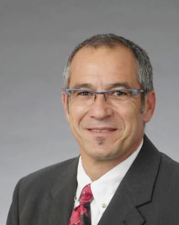
Interview 7: Professor John Bowers
August has been a notable month for John Bowers.
Juniper Networks announced its intention to acquire Aurrion, the US silicon photonics start-up that Bowers co-founded with Alexander Fang. And Intel, a company Bowers worked with on a hybrid integration laser-bonding technique, unveiled its first 100-gigabit silicon photonics transceivers.
 Professor John BowersBower, a professor in the Department of Electrical and Computer Engineering at the University of California, Santa Barbara (UCSB), first started working in photonics in 1981 while at AT&T Bell Labs.
When he became interested in silicon photonics, it still lacked a good modulator and laser. "If you don't have a laser and a modulator, or a directly modulated laser, it is not a very interesting chip,” says Bowers. "So I started thinking how to do that."
Bowers contacted Mario Paniccia, who headed Intel’s silicon photonics programme at the time, and said: “What if we can integrate a laser? I think there is a good way to do it.” The resulting approach, known as heterogeneous integration, is one that both Intel and Aurrion embraced and since developed.
This is a key Bowers trait, says Aurrion co-founder, Fang: he just knows what problems to work on.
"John came up with the concept of the hybrid laser very early on," says Fang. "Recall that, at that time, silicon photonics was viewed as nothing more than people making plasma-effect phase shifters and simple passive devices. John just cut to the chase and went after combining III-V materials with silicon."
If you look at the major companies with strong photonics activities, you’ll find a leader in that group that was developed under John’s training
Fang also highlights Bowers' management skills. “John can pick players and run teams,” says Fang, who describes himself as one of those privileged to graduate out of Bowers’ research group at UCSB.
“You find yourself in an environment where John picks a team of sharp folk with complementary skills and domain expertise to solve a problem that John determines as important and has some insight on how to solve it,” says Fang. “If we look like we are going to drive off the road, he nudges with a good mix of insight, fear, and humour.”
It has resulted in some of the best trained independent thinkers and leaders in the industry, says Fang: “If you look at the major companies with strong photonics activities, you’ll find a leader in that group that was developed under John’s training”.
Silicon photonics
Bowers defines silicon photonics as photonic devices on a silicon substrate fabricated in a CMOS facility.
“Silicon photonics is not about using silicon for everything; that misses the point,” says Bowers. “The key element is using silicon as a substrate - 12-inch wafers and not 2- or 3-inch wafers - and having all the process capability a modern silicon CMOS facility brings.” These capabilities include not just wafer processing but also advanced testing and packaging.
The world is about to change and I don't think people have quite figured that out
“If you go to an advanced packaging house, they don't do 6-inch wafers and I don't know of indium phosphide and gallium arsenide wafers larger than 6 inches,” says Bowers. “The only solution is to go to silicon; that is the revolution that hasn't happened yet but it is happening now.”
Bowers adds that everything Aurrion does, there is automated test along the way. "And I think you have others; Luxtera has done a great job as well at wafer-level test and packaging," he says. "The world is about to change and I don't think people have quite figured that out."
Working with Intel was an eye-opener for Bowers, especially the process controls it applies to chip-making.
“They worry about distributions and yields, and it is clear why there are seven billion transistors on a chip and that chip will yield,” says Bowers. “When you apply that to photonics, it will take it to a whole new level.” Indeed, Bowers foresees photonics transfering to silicon.
Bowers highlights the fairly complex chips now being developed using silicon photonics.
“We have done a 2D scanner - a 32-element phased array - something one could never do in optics unless it was integrated all on one chip,” he says. The phased-array chip comprises 160 elements and is physically quite large.
This is another benefit of using 12-inch silicon wafers and fabricating the circuits in a CMOS facility. “You are not going to cost-effectively do that in indium phosphide, which I've worked on for the last 30 years,” says Bowers.
Another complex device developed at UCSB is a 2.54-terabit network-on-a-chip. “This is a larger capacity than anyone has done on any substrate,” he says.
Infinera’s latest photonic integrated circuit (PIC), for example, has a transport capacity of up to 2.4 terabit-per-second. That said, Bowers stresses that the network-on-a-chip is a research presentation while Infinera’s PIC is a commercial device.
Heterogeneous integration
Heterogeneous integration involves bonding materials such as III-V compounds onto silicon.
Bowers first worked on III-V bonding with HP to make longer wavelength - 1310nm and 1550nm - VCSELs. “We had been bonding indium phosphide and gallium arsenide to solve a fundamental problem that indium phosphide does not make good mirrors,” he says. “So I was pretty confident we could bond III-V to silicon to add gain to silicon photonics to then add all the laser capability.”
Bonding to silicon is attractive as it enables the integration of optical features that haven't been widely integrated onto any other platform, says Bowers. These include not only lasers but other active devices such as modulators and photo-detectors, as well as passive functions such as isolators and circulators.
One concern raised about heterogeneous integration and the use of III-V materials is the risk of contamination of a CMOS fabrication line.
Bowers points out that the approached used does not impact the front end of the fabrication, where silicon wafers are etched and waveguides formed. The III-V material is bonded to the wafer at the fab’s back end, the stage where metallisation occurs when making a CMOS chip.
The leading chipmakers are also experimenting with III-V materials to create faster digital devices due to their higher electron mobility. “This is part of the natural evolution of CMOS,” he says. It remains unclear if this will be adopted, but it is possible that a 5nm CMOS node will use indium phosphide.
“All the CMOS houses are doing lots of work on III-V and silicon,” says Bowers. “They have figured out how to control that contamination issue.”
New capabilities
Bowers and his team have already demonstrated the integration of new optical functions on silicon.
“Neither silicon nor indium phosphide has an isolator and one always has to use an external YIG (yttrium iron garnet) isolator to reduce the reflection sensitivity of things like widely tunable lasers,” says Bower.
His team has developed a way to bond a YIG onto silicon using the same techniques it uses for bonding III-V materials. The result is an integrated isolator device with 32dB isolation and a 2dB insertion loss, a level of performance matching those of discrete isolators.
Incorporating such functionality onto silicon creates new possibilities. “We have a paper coming out that features a 6-port circulator,” says Bowers. “It is not a tool that the community can use yet because it has never been made before but we can do that on silicon now,” he says. “That is a good new capability.”
Superior performance
Bowers stresses that heterogeneous integration can also result in optical performance superior to a III-V design alone. He cites as an example how using a silicon nitride waveguide, with its lower loss that indium phosphide or gallium arsenide, can create high-quality Q-resonators.
A Q-resonator can be viewed as a form of filter. Bowers' group have demonstrated one with a Q of 80 million. “That makes it very sensitive to a variety of things,” he says. One example is for sensors, using a Q resonator with a laser and detector to form a spectrometer.
His researchers have also integrated the Q resonator with a laser to make a widely tunable device that has a very narrow line-width: some 40kHz wide. This is a narrower than the line-width of commercially-available tunable lasers and exceeds what can be done with indium phosphide alone, he says.
Challenges
Bowers, like other silicon photonics luminaries, highlights the issues of automated packaging and automated testing, as important challenges facing silicon photonics. “Taking 10,000s of transceivers and bringing all the advanced technology - not just processing but test and packaging - that are being developed for cell phones,” he says.
Too much of photonics today is based on gold boxes and expensive transceivers. “Where Aurrion and Intel are going is getting silicon photonics to the point where photonics will be ubiquitous, cheap and high yielding,” he says. This trend is even evident with his university work. The 400-element 2.54-terabit network-on-a-chip has very high laser yields, as are its passive yields, he says.
“So, effectively, what silicon photonics can do is going up very rapidly,“ says Bowers. “If you can put it in the hands of a real CMOS player like Intel or the companies that Aurrion uses, it is going to take photonics to a whole new area that people would not have thought possible in terms of complexity.”
Yet Bowers is also pragmatic. “It still takes time,” he says. “You can demonstrate an idea, but it takes time to make it viable commercially.”
He points to the recently announced switch from Oracle that uses mid-board optics. “That is a commercial product out there now,” he says. “But is it silicon photonics? No, it is VCSEL-based; that is the battle going on now.”
VCSELs have won the initial battle in the data centre but the amount of integration the technology can support is limited. Once designers move to wavelength-division multiplexing to get to higher capacities, where planar technology is required to combine and separate the different wavelengths efficiently, that is when silicon has an advantage, he says.
The battle at 100 gigabit between VCSELs and silicon photonics is also one that Bowers believes silicon photonics will eventually win. But at 400 gigabit and one terabit, there is no way to do that using VCSELs, he says.
Status
The real win for silicon photonics is when optics moves from transceivers at the edge of the board to mid-board and eventually are integrated with a chip in the same package, he says.
Advanced chips such as switch silicon for the data centre are running into an input-output problem. There are only so many 25 gigabit-per-second signals a chip can support. Each signal, sent down a trace on a printed circuit board, typically requires equalisation circuitry at each end and that consumes power.
Most of the photonics industry has focused on telecom and datacom, and justifiably so. The next big thing will happen in the area of sensors.
A large IC packaged as a ball grid array may have as many as 5,000 bumps (balls) that are interfaced to the printed circuit board. Using photonics can boost the overall bandwidth coming on and off the chip.
“With photonics, and in particular when we integrate the laser as well as the modulator, the world doesn't see it as a photonics chip, it's an electronics chip, it just turns out that some of those bumps are optical ones and they provide much more efficient transmission of data and at much lower power,” say Bowers. A 100 terabit of even a 1000 terabit - a petabit - switch chip then becomes possible. This is not possible electrically but it is possible by integrating photonics inside the package or on the chip itself, he says.
“That is the big win eventually and that is where we help electronics extend Moore’s law,” says Bowers.
And as silicon photonics matures, other applications will emerge - More than Moore’s law - like the use of photonics for sensors.
“Most of the photonics industry has focused on telecom and datacom, and justifiably so,” says Bowers. “The next big thing will happen in the area of sensors.”
Professor Bowers was interviewed before the Juniper Networks announcement
Intel's 100-gigabit silicon photonics move
Intel has unveiled two 100-gigabit optical modules for the data centre made using silicon photonics technology.
 Alexis Bjorlin
The PSM4 and CWDM4/CLR4 100-gigabit modules mark the first commercial application of a hybrid integration technique for silicon photonics, dubbed heterogeneous integration, that Intel has been developing for years.
Intel's 100-gigabit module announcement follows the news that Juniper Networks has entered into an agreement to acquire start-up, Aurrion, for $165 million. Aurrion is another silicon photonics player developing this hybrid integration technology for its products.
Hybrid integration
With heterogeneous integration, materials such as indium phosphide and gallium arsenide can be bonded to the silicon substrate before the 300mm wafer is processed to produce the optical circuit. Not only can lasers be added to silicon but other active devices such as modulators and photo-detectors as well as passive functions such as isolators and circulators.
There is no alignment needed; we align the laser with lithography
Intel is using the technique to integrate the laser as part of the 100-gigabit transceiver designs.
"Once we apply the light-emitting material down to the silicon base wafer, we define the laser in silicon," says Alexis Bjorlin, vice president and general manager, Intel Connectivity Group. “There is no alignment needed; we align the laser with lithography.”
Intel claims it gets the highest coupling efficiency between the laser and the optical waveguide and modulator because it is lithographically defined and requires no further alignment.
100-gigabit modules
Intel is already delivering the 100-gigabit PSM4 module. “First volume shipments are happening now,” says Bjorlin. Microsoft is one Internet content provider that is using Intel’s PSM4.
The chip company is also sampling a 100-gigabit CWDM4 module that also meets the more demanding CLR4 Alliance’s optical specification. The 100-gigabit CLR4 module can be used without forward-error correction hardware and is favoured for applications where latency is an issue such as high-performance computing.
Intel is not the first vendor to offer PSM4 modules, nor is it the first to use silicon photonics for such modules. Luxtera and Lumentum are shipping silicon photonics-based PSM4 modules, while STMicroelectronics is already supplying its PSM4 optical engine chip.
We are right on the cusp of the real 100-gigabit connectivity deployments
“Other vendors have been shipping PSM4 modules for years, including large quantities at 40 gigabit,” says Dale Murray, principal analyst at LightCounting Market Research. “Luxtera has the clear lead in silicon photonics-based PSM4 modules but a number of others are shipping them based on conventional optics.”
The PSM4 is implemented using four independent 25-gigabit channels sent over a single-mode ribbon fibre. Four fibres are used for transmission and four fibres for receive.
“The PSM4 configuration is an interesting design that allows one laser to be shared among four separate output fibres,” says Murray. “As Luxtera has shown, it is an effective and efficient way to make use of silicon photonics technology.”
The CWDM4 is also a 4x25-gigabit design but uses wavelength-division multiplexing and hence a single-mode fibre pair. The CWDM4 is a more complex design in that an optical multiplexer and demultiplexer are required and the four lasers operate at different wavelengths.
“While the PSM4 module does not break new ground, Intel’s implementation of WDM via silicon photonics in a CWDM4/CLR4 module could be more interesting in a low-cost QSFP28 module,” says Murray. WDM-based QSFP28 modules are shipping from a number of suppliers that are using conventional optics, he says.
Intel is yet to detail when it will start shipping the CWDM4/CLR4 module.
Market demand
Bjorlin says the PSM4 and the CWDM4/CLR4 will play a role in the data centre. There are applications where being able to break out 100-gigabit into 25-gigabit signals as offered by the PSM4 is useful, while other data centre operators prefer a duplex design due to the efficient use of fibre.
“We are right on the cusp of the real 100-gigabit connectivity deployments,” she says.
As for demand, Bjorlin expects equal demand for the two module types in the early phases: “Longer term, we will probably see more demand for the duplex solution”.
LightCounting says that 100-gigabit PSM4 modules took an early lead in the rollout of 100 Gigabit Ethernet, with VCSEL-based modules not far behind.
“Some are shipping CWDM4/CLR4 and we expect that market to ramp,” says Murray. “Microsoft and Amazon Web Services seem to like PSM4 modules while others want to stick with modules that can use duplex fibre.
 Source: Intel
Data centre switching
“One of the most compelling reasons to drive silicon photonics in the future is that it is an integratable platform,” says Bjorlin.
Switch silicon from the likes of Broadcom support 3.2 terabits of capacity but this will increase to 6.4 terabits by next year and 12.8 terabits using 4-level pulse amplitude modulation (PAM-4) signalling by 2018 (see chart). And by 2020, 25.6-terabit capacity switch chips are expected.
The demand for 100 gigabit is for pluggable modules that fit into the front panels of data center switches. But the market is evolving to 400-gigabit embedded optics that sit on the line card, she says, to enable these emerging higher-capacity switches. Intel is a member of the Consortium of On-Board Optics (COBO) initiative that is being led by Microsoft.
“When you get to 25.6-terabit switches, you start to have a real problem getting the electrical signals in and out of the switch chip,” says Bjorlin. This is where silicon photonics can play a role in the future by co-packaging the optics alongside the switch silicon.
“There will be a need for an integrated solution that affords the best power consumption, the best bandwidth-density that we can get and effectively position silicon photonics for optical I/O [input/output],” says Bjorlin. “Ultimately, that co-packaging is inevitable.”
Juniper Networks to acquire Aurrion for $165 million
The announcement of the acquisition was low key. A CTO blog post and a statement that Juniper Networks had entered into an agreement to acquire Aurrion, the fabless silicon photonics start-up. No fee was mentioned.
However, in the company's US Securities and Exchange Commission filing, Juniper values the deal at approximately $165 million. "The Company believes the acquisition will help to fuel its long-term competitive advantage by enabling cost-effective, high-density, high-speed optical networks," it said. The deal is expected to be closed this quarter.

But the deal is significant for a number of reasons.
First, Aurrion, like Intel, is a proponent of heterogeneous integration, combining indium phosphide and other technologies on a silicon wafer platform through bonding. The approach has still to be proven in commercial volumes but it promises the use of III-V materials on 12-inch silicon wafers manufactured in a chip fabrication plant.
Aurrion has made tunable lasers for telecom that cover both the C- and L-bands, as well as uncooled laser arrays for datacom applications. The start-up has also been developing high-speed transceivers for the data centre.
The company has also been working on the manufacturing aspects of silicon photonics, a considerable undertaking. These include automated wafer-scale testing, connecting fibre to a silicon photonics chip, and packaging.
Juniper is thus getting an advanced silicon photonics technology suited for volume manufacturing that it will use to advance its data centre networking offerings.
Juniper may choose to make its own optical transceivers but, more likely, it will use silicon photonics as part of its switch designs to tackle issues of data centre scaling and the continual challenge of growing power consumption. It could also use the technology for its IP core routers and longer term, to tackle I/O issues alongside custom ASICs.
Systems vendors drive silicon photonics
The Aurrion acquisition also highlights how it is systems vendors that are acquiring silicon photonics start-ups rather than the traditional optical component and module makers.
This is partly a recognition that silicon photonics' main promise is as a systems technology. Acacia, the coherent transmission specialist, is one company that has shown how silicon photonics can benefit optical module design but the technology's longer-term promise is for systems design rather than optical modules.
A consequence of such acquisitions by systems vendors is that technology being developed by silicon-photonics start-ups is being swallowed within systems houses for their own use and not for the merchant market. Systems vendors have deep pockets to develop the technology but it will be for their own use. For the wider community, silicon photonics technology being developed by the likes of Aurrion is no longer available.
This is what AIM Photonics, the US public-private partnership that is developing technology for integrated photonics, is looking to address: to advance the manufacturing of silicon photonics, making the resulting technology available to small to medium sized businesses and entrepreneurial ventures. However, AIM Photonics is one year into a five-year venture.
Implications
Should major systems vendors owning silicon photonics technology in-house concern the traditional optical component vendors?
Not for now.
Optical transceiver sales continue to grow and the bulk of designs are not integrated. And while silicon photonics is starting to be used for integrated designs, it is competing against the established technologies of indium phosphide and gallium arsenide.
But as photonics moves closer to the silicon and away from a system's faceplate, silicon photonics becomes more strategically important and this is where systems vendors can start developing custom designs.
Must the systems houses own the technology to do that?
Not necessarily, but they will need silicon photonics design expertise, and in the case of Juniper, it can hit the ground running with Aurrion.
Longer term, it will be the much larger chip industry that will drive silicon photonics rather than the optical industry. There are chip foundries now that are making silicon photonic ICs as there are top-ten chip companies such as Intel and STMicroelectronics. But ultimately it will be a very different supply chain that will take shape.
It is early days but Juniper's acquisition is the latest indicator that it is the systems vendors that are moving first at the very beginnings of this new ecosystem.
The ecosystem for silicon photonics starts to take shape
Silicon photonics luminaries series
Interview 6: imec - Philippe Absil and Joris Van Campenhout
Imec has a unique vantage point when it comes to the status and direction of silicon photonics.
The Belgium nano-electronics research centre gets to see prototype designs nearing commercialisation due to its silicon photonics integration platform and foundry service. “We allow companies to build prototypes using a robust silicon photonics technology,” says Philippe Absil, department director for 3D and optical technologies at imec.
 Philippe Absil
Imec also works intimately with several partners on longer-term research, one being Huawei. This optical I/O R&D activity is part of imec’s CORE CMOS scaling R&D programme which as well as Huawei includes GlobalFoundries, Intel, Micron, Qualcomm, Samsung, SK Hynix, Sony and TSMC. The research is sufficiently far ahead to be deemed pre-competitive such that all the firms collaborate.
For silicon photonics, the optical I/O research includes optical integration schemes, new device concepts and new materials. “The aim is to bring silicon photonics technology to the next level in order to resolve today’s challenges,” says Absil.
Assured future
Imec is confident about silicon photonics’ future but stresses an ecosystem for the technology needs to be in place first. This means having more than one foundry, suitable equipment to reduce the cost of testing silicon photonics circuits, and developing packaging solutions.
“These elements are being developed and the ecosystem is coming together nicely,” says Joris Van Campenhout, programme director for optical I/O at imec.
Another encouraging sign is the strong industry interest in the technology in the last two years. It was mainly academics that were interested in imec's multi-wafer project service but now there is strong demand from companies as well; companies bringing products to market.
Silicon photonics is not a one-off technology; it has value for several generations
Systems scaling is what gives imec confidence that silicon photonics will not end up a niche technology. “Look at the cloud economy and cloud data centres, these systems need to scale continually,” says Van Campenhout. “A lot of effort is being put into scaling, and interconnect is an essential part of such systems.”
Moreover, there are few technologies to deliver such scalability, which is why many of the bigger systems companies are investing in silicon photonics. “Silicon photonics is not a one-off technology; it has value for several generations," says Van Campenhout. “That is really the potential of silicon photonics and that is where the disruption lies.”
Challenges
One focus for imec and its partners is to reduce the overall insertion loss of silicon photonics circuits for short-reach interconnect applications. Such short-reach links span distances of up to a few meters, a market segment currently addressed using advanced copper cabling or VCSEL-based optical interconnects.
 Joris Van Campenhout
Because of the relatively high insertion loss of silicon photonics designs, it is not possible to achieve a sufficiently low-power consumption for such links. “That is a show-stopper because it prevents us closing link budgets,” says Van Campenhout. A link budget refers to the gain and losses across the elements making up the optical link such as the laser, modulator, optical fibre and receiver circuitry.
In order to drive up volumes, silicon photonics needs to become more competitive at shorter reaches where VCSELs are still the mainstream optical technology
The team is tackling the loss issue on two fronts: reducing the insertion loss between the fibre and the waveguide, and reducing the modulator's insertion loss which still exceeds that of other optical technologies.
“For these two parts of the technology, further improvements are required to reduce the overall losses,” says Van Campenhout. “That will enable us to be competitive at shorter distances.” These are engineering challenges, he stresses, rather than any fundamental problem.
Another silicon photonics research area being explored at imec include edge coupling solutions between the waveguide and fibre. “These can have very low insertions losses - one decibel or lower - and can be polarisation insensitive," says Van Campenhout.
Packaging approaches that have a low insertion loss are also being developed, engineered in a way to enable passive alignment assembly procedures. Passively aligning the laser is a key part of reducing component packaging costs. “Silicon doesn’t have a laser so in the next few years it will continue to require hybrid solutions,” says Van Campenhout. “You need a good way to do passive alignment of laser sources, and also packaged in a way that doesn’t require a hermetic solution.”
These are the challenges facing the industry in the next few years: lowering insertion loss and developing packaging technologies. Overcoming these challenges will mark an important milestone since the total market for silicon photonics can be served with a small number of silicon wafers. “In order to drive up volumes, silicon photonics needs to become more competitive at shorter reaches where VCSELs are still the mainstream optical technology,” says Van Campenhout.
It is not yet mature but there is a broader adoption of a model whereby silicon photonics can be designed by one company and fabricated by another
Value proposition
Overall, silicon photonics faces stiff competition from VCSELs and indium phosphide. The two established optical technologies continue to evolve and benefit from having all the optical functionality in one platform, something that silicon photonics, with its lack of a laser source, can’t match.
But the trend whereby the optical transceiver is coming ever closer to the host IC strengthens silicon photonics’ hand. That is because silicon photonics can be co-packaged with silicon, and can share the same equipment as the two device types - electronic and photonic ICs - are put together.
Absil also highlights how the ecosystem needed for widespread adoption of silicon photonics is taking shape. “It is not yet mature but there is a broader adoption of a model whereby silicon photonics can be designed by one company and fabricated by another,” he says. “The adoption of that will result in a new model for the optical component world.”
Market opportunities
Van Campenhout expects silicon photonics to be a niche technology for 100-gigabit connections in the data centre. This may change as silicon photonics matures but today the market is dominated by III-V technologies, he says.
Applications that require integration density in the form of a large number of parallel high-speed transceivers, and close integration with host ICs is what will drive silicon photonics. Imec cites as an example data centre switches which require a large number of network and backplane interconnects tightly integrated with the switch logic IC. These interconnects will be on-board and eventually on-package optical modules. Silicon photonics is ideally placed to provide a scalable I/O solution for such applications, as channel data rates move to 50 gigabit and beyond, says Van Campenhout.
But if it is going to take several years to resolve the insertion loss issues for short-reach interconnects, this is a market application that will only start driving significant volumes early in the next decade.
The advent of 400 Gigabit Ethernet and perhaps 800 Gigabit Ethernet after that will be another driver in the coming years.
Other emerging markets include sensors. “Mid infra-red for sensing is a very interesting topic with quite some potential,” says Van Campenhout. “But it is not entirely clear what will be the killer application.”
Sensing is a fragmented application area where many technology solutions exist. “It is too early to figure out what applications an optical sensing device would be competitive against incumbent designs.” But the more integration required, the more competitive silicon photonics will become for such applications, he says.
The Internet of Things will also use sensing but this will be an extremely cost-sensitive market.
“It is not entirely clear if optical technology will be able to meet such cost pressures but if it does, it will drive tremendous volumes and help develop an ecosystem around silicon photonics,” says Van Campenhout.
Further reading:
Imec gears up for the Internet of Things economy, click here
ST makes its first PSM4 optical engine deliveries
What gives Benetti confidence is the demand he is seeing for 100-gigabit transceivers in the data centre. “From my visibility today, the tipping point is 2016,” says Benetti, group vice president and general manager, digital and mixed processes ASIC division at STMicroelectronics.
 Flavio Benetti
Benetti and colleagues at ST have spent the last four years working to bring to market the silicon photonics technology that the chip company licensed from Luxtera.
The company has developed a 300mm-wafer silicon photonics production line at its fabrication plant in Crolles that is now up and running. ST also has its first silicon photonics product - a mid-reach PSM4 100-gigabit optical engine - and has just started its very first deliveries.
At the OFC show in March, ST said it had already delivered samples to one unnamed 'customer partner', possibly Luxtera, and Benetti showed a slide of the PSM4 chips as part of a Lumentum transceiver.
Another ST achievement Benetti highlights is the development of a complete supply chain for the technology. In addition to wafer production, ST has developed electro-optic wafer testing. This allows devices to be probed electrically and optically to select working designs before the wafer is diced. ST has also developed a process to 3D-bond chips.
“We have focussed on building an industrial environment, with a supply chain that can deliver hundreds of thousands and millions of devices,” says Benetti.
PSM4 and CWDM4
ST’s first product, the components for a 4x25 gigabit PSM4 transceiver, is a two-chip design.
One chip is the silicon photonics optical engine which integrates the PSM4’s four modulators, four detectors and the grating couplers used to interface the chip to the fibres. The second chip, fabricated using ST’s 55nm BiCMOS process, houses the transceiver’s associated electronics such as the drivers, and trans-impedance amplifiers.
The two chips are combined using 3D packaging. “The 3D packaging consists of the two dies, one copper-pillar bonded to the other,” says Benetti. “It is a dramatic simplification of the mounting process of an optical module.”
The company is also developing a 100-gigabit CWDM4 transceiver which unlike the PSM4 uses four 25-gigabit wavelengths on a single fibre.
The CWDM4 product will be developed using two designs. The first is an interim, hybrid solution that uses an external planar lightwave circuit-based multiplexer and demultiplexer, followed by an integrated silicon photonics design. The hybrid design is being developed and is expected in late 2017; the integrated silicon photonics design is due in 2018.
With the hybrid design, it is not just a question of adding a mux-demux to the PSM4 design. “The four channels are each carrying a different wavelength so there are some changes that need to be done to the PSM4,” says Benetti, adding that ST is working with partners that will provide the mux-demux and do the integration.
We need to have a 100-gigabit solution in high volume for the market, and the pricing pressure that is coming has convinced us that silicon photonics is the right thing to do
Opportunities
Despite the growing demand for 100-gigabit transceivers that ST is seeing, Benetti stresses that these are not 'mobile-phone wafer volumes'. “We are much more limited in terms of wafers,” he says. Accordingly, there is probably only room for one or two large fabs for silicon photonics globally, in his opinion.
So why is ST investing in a large production line? For Benetti, this is an obvious development for the company which has been a provider of electrical ICs for the optical module industry for years.
“ST has entered silicon photonics to provide our customers with a roadmap,” says Benetti. “We need to have a 100-gigabit solution in high volume for the market, and the pricing pressure that is coming has convinced us that silicon photonics is the right thing to do.”
It also offers chip players the possibility of increasing its revenues. “The optical engine integrates all the components that were in the old-fashioned modules so we can increase our revenues there,” he says.
ST is tracking developments for 200-gigabit and 400-gigabit links and is assessing whether there is enough of an opportunity to justify pursuing 200-gigabit interconnects.
For now though, it is seeing strong pricing pressure for 100-gigabit links for reaches of several hundred meters. “We do not think we can compete for very short reach distances,” says Benetti. “We will leave that to VCSELs until the technology can no longer follow.” As link speeds increase, the reach of VCSEL links diminishes. “We will see more room for silicon photonics but this is not the case in the short term,” says Benetti.
Market promise
People have been waiting for years for silicon photonics to become a reality, says Benetti. “My target is to demonstrate it [silicon photonics] is possible, that we are serious in delivering parts to the market in an industrial way and in volumes that have not been delivered before.”
To convince the market, it is not just showing the technological advantages of silicon photonics but the fact that there is a great simplification in constructing the optical module along with the ability to deliver devices in volume. “This is the point,” he says.
Benetti’s other role at ST is overseeing advanced networking ASICs. He argues that over the mid- to long-term, there needs to be a convergence between ASIC and optical connectivity.
“Look at a switch board, for example, you have a big ASIC or two in the middle and a bunch of optical modes on the side,” says Benetti. For him, the two technologies - photonics and ICs - are complementary and the industry’s challenge is to make the two live together in an efficient way.
FPGAs with 56-gigabit transceivers set for 2017
The company demonstrated a 56-gigabit transceiver using 4-level pulse-amplitude modulation (PAM-4) at the recent OFC show. The 56-gigabit transceiver, also referred to as a serialiser-deserialiser (serdes), was shown successfully working over backplane specified for 25-gigabit signalling only.
 Gilles GarciaXilinx's 56-gigabit serdes is implemented using a 16nm CMOS process node but the first FPGAs featuring the design will be made using a 7nm process. Gilles Garcia says the choice of 7nm CMOS is solely a business decision and not a technical one.
”Optical module [makers] will take another year to make something decent using PAM-4," says Garcia, Xilinx's director marketing and business development, wired communications. "Our 7nm FPGAs will follow very soon afterwards.”
The company is still to detail its next-generation FPGA family but says that it will include an FPGA capable of supporting 1.6 terabit of Optical Transport Network (OTN) using 56-gigabit serdes only. At first glance that implies at least 28 PAM-4 transceivers on a chip but OTN is a complex design that is logic not I/O limited suggesting that the FPGA will feature more than 28, 56-gigabit serdes.
Applications
Xilinx’s Virtex UltraScale and its latest UltraScale+ FPGA families feature 16-gigabit and 25-gigabit transceivers. Managing power consumption and maximising reach of the high-speed serdes are key challenges for its design engineers. Xilinx says it has 150 engineers for serdes design.
“Power is always a key challenge because as soon as you talk about 400-gigabit to 1-terabit per line card, you need to be cautious about the power your serdes will use,” says Garcia. He says the serdes need to adapt to the quality of the traces for backplane applications. Customers want serdes that will support 25 gigabit on existing 10-gigabit backplane equipment.
Xilinx describes its Virtex UltraScale as a 400-gigabit capable single-chip system supporting up to 104 serdes: 52 at 16 gigabit and 52 at 25 gigabit.
The UltraScale+ is rated as a 500-gigabit to 600-gigabit capable system, depending on the application. For example, the FPGA could support three, 200-gigabit OTN wavelengths, says Garcia.
Xilinx says the UltraScale+ reduces power consumption by 35% to 50% compared to the same designs implemented on the UltrasScale. The Virtex UltraScale+ devices also feature dedicated hardware to implement RS-FEC, freeing up programmable logic for other uses. RS-FEC is used with multi-mode fibre or copper interconnects for error correction, says Xilinx. Six UltraScale+ FPGAs are available and the VU13P, not yet out, will feature up to 128 serdes, each capable of up to 32 gigabit.
We don’t need retimers so customers can connect directly to the backplane at 25 gigabit, thereby saving space, power and cost
The UltraScale and UltraScale+ FPGAs are being used in several telecom and datacom applications.
For telecom, 500-gigabit and 1-terabit OTN designs are an important market for the UltraScale FPGAs. Another use for the FPGA serdes is for backplane applications. “We don’t need retimers so customers can connect directly to the backplane at 25 gigabit, thereby saving space, power and cost,” says Garcia. Such backplane uses include OTN platforms and data centre interconnect systems.
The FPGA family’s 16-gigabit serdes are also being used in 10-gigabit PON and NG-PON2 systems. “When you have an 8-port or 16-port system, you need to have a dense serdes capability to drive the [PON optical line terminal’s] uplink,” says Garcia.
For data centre applications, the FPGAs are being employed in disaggregated storage systems that involved pooled storage devices. The result is many 16-gigabit and 25-gigabit streams accessing the storage while the links to the data centre and its servers are served using 100-gigabit links. The FPGA serdes are used to translate between the two domains (see diagram).
 Source: Xilinx
For its next-generation 7nm FPGAs with 56-gigabit transceivers, Xilinx is already seeing demand for several applications.
Data centre uses include server-to-top-of-rack links as the large Internet providers look move from 25 gigabit to 50- and 100-gigabit links. Another application is to connect adjacent buildings that make up a mega data centre which can involve hundreds of 100-gigabit links. A third application is meeting the growing demands of disaggregated storage.
For telecom, the interest is being able to connect directly to new optical modules over 50-gigabit lanes, without the need for gearbox ICs.
Optical FPGAs
Altera, now part of Intel, developed an optical FPGA demonstrator that used co-packaged VCSELs for off-chip optical links. Since then Altera announced its Stratix 10 FPGAs that include connectivity tiles - transceiver logic co-packaged and linked with the FPGA using interposer technology.
Xilinx says it has studied the issue of optical I/O and that there is no technical reason why it can’t be done. But the issue is a business one when integrating optics in an FPGA, he says: “Who is responsible for the yield? For the support?”
Garcia admits Xilinx could develop its own I/O designs using silicon photonics and then it would be responsible for the logic and the optics. “But this is not where we are seeing the business growing,” he says.
Enabling coherent optics down to 2km short-reach links
Interview 5: Chris Doerr
Chris Doerr admits he was a relative latecomer to silicon photonics. But after making his first silicon photonics chip, he was hooked. Nearly a decade later and Doerr is associate vice president of integrated photonics at Acacia Communications. The company uses silicon photonics for its long-distance optical coherent transceivers.
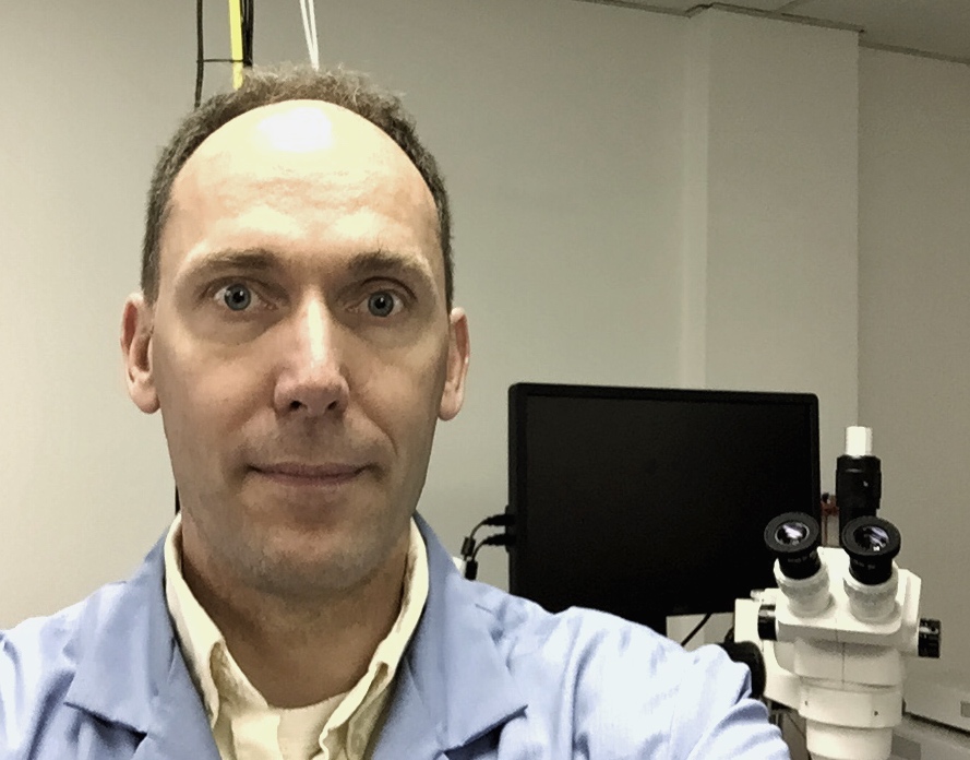 Chris Doerr in the lab
Acacia Communications made headlines in May after completing an initial public offering (IPO), raising approximately $105 million for the company. Technology company IPOs have become a rarity and are not always successful. On its first day of trading, Acacia’s shares opened at $29 per share and closed just under $31.
Although investors may not have understood the subtleties of silicon photonics or coherent DSP-ASICs for that matter, they noted that Acacia has been profitable since 2013. But as becomes clear in talking to Doerr, silicon photonics plays an important role in the company’s coherent transceiver design, and its full potential for coherent has still to be realised.
Bell Labs
Doerr was at Bell Labs for 17 years before joining Acacia in 2011. He spent the majority of his time at Bell Labs making first indium phosphide-based optical devices and then also planar lightwave circuits. One of his bosses at Bell Labs was Y.K. Chen. Chen had arranged a silicon photonics foundry run and asked Doerr if he wanted to submit a design.
What hooked Doerr was silicon photonics’ high yields. He could assume every device was good, whereas when making complex indium phosphide designs, he would have to test maybe five or six devices before finding a working one. And because the yields were high, he could focus more on the design aspects. “Then you could start to make very complex designs - devices with many elements - with confidence,” he says.
Another benefit was that the performance of the silicon photonic circuit matched closely its simulation results. “Indium phosphide is so complex,” he says. “You have to worry about the composition effects and the etching is not that precise.” With silicon, in contrast, the dimensions and the refractive index are known with precision. “You can simulate and design very precisely, which made it [the whole process] richer,” says Doerr.
Silicon photonics is a disruptive technology because of its ability to integrate so many things together and still be high yield and get the raw performance
After that first wafer run, Doerr continued to design both planar lightwave circuits and indium phosphide components at Bell Labs. But soon it was solely silicon photonics ICs.
Doerr views Acacia’s volume production of an integrated coherent transceiver - the transmit and receive optics on the one chip - with a performance that matches discrete optical designs, as one of silicon photonics’ most notable achievements to date.
With a discrete component coherent design, you can use the best of each material, he explains, whereas with an integrated design, compromises are inevitable. “You can’t optimise the layer structure; each component has to share the wafer structure,” he says. Yet with silicon photonics, the design space is so powerful and high-yielding, that these compromises are readily overcome.
Doerr also describes a key moment when he realised the potential of silicon photonics for volume manufacturing.
He was reading an academic paper on grating couplers, a structure used to couple fibres to waveguides. “You can only make that in silicon photonics because you need a high vertical [refractive] index contrast,” he says. Technically, a grating coupler can also be made in indium phosphide but the material has to be cut from under the waveguide; this leaves the waveguide suspended in air.
When he first heard of grating couplers he assumed the coupling efficiency would be of the order of a few percent whereas in practice it is closer to 85 percent. “That is when I realised it is a very powerful concept,” he says.
Integration is key
Doerr pauses before giving measured answers to questions about silicon photonics. Nor does his enthusiasm for silicon photonics blinker him to the challenges it faces. However, his optimism regarding the technology’s future is clear.
“Silicon photonics is a disruptive technology because of its ability to integrate so many things together and still be high yield and get the raw performance,” he says. In the industry, silicon photonics has proven itself for such applications as metro telecommunications but it faces significant competition from established technologies such as indium phosphide. It will require more channels to be integrated for the full potential of silicon photonics as a disruption technology to emerge, says Doerr.
Silicon photonics also has an advantage on indium phosphide in that it can be integrated with electronic ICs using 2.5D and 3D packaging, saving cost, footprint, and power. “If you are in the same material system then such system-in-package is easier,” he says. Also, silicon photonic integrated circuits do not require temperature control, unlike indium phosphide modulators, which saves power.
Areas of focus
One silicon photonics issue is the need for an external laser. For coherent transceivers, it is better to separate the laser from the high-speed optics due to the fact that the coherent DSP-ASIC and the photonic chips are hot and the laser requires temperature control.
For applications such as very short reach links, silicon photonics needs a laser source and while there are many options to integrate the laser to the chip, a clear winning approach has yet to emerge. “Until a really low cost solution is found, it precludes silicon from competing with really low-cost solutions like VCSELs for very short reach applications,” he says.
Silicon photonic chip volumes are still many orders of magnitude fewer than those of electronic ICs. But Acacia says foundries already have silicon photonics lines running, and as these foundries ramp volumes, costs, production times, and node-sizes will continually improve.
Opportunities
The adoption of silicon photonics will increase significantly as more and more functions are integrated onto devices. For coherent designs, Doerr can foresee silicon photonics further reducing the size, cost and power consumption, making them competitive with other optical transceiver technologies for distances as short as 2km.
“You can use high-order formats such as 256-QAM and achieve very high spectral efficiency,” says Doerr. Using such a modulation scheme would require fewer overall lasers to achieve significant transport capacities, improving the cost-per-bit performance for applications such as data centre interconnect. “Fibre is expensive so the more you can squeeze down a fibre, the better,” he says.
Doerr also highlights other opportunities for silicon photonics, beyond communications. Medical applications is one such area. He cites a post-deadline paper at OFC 2016 from Acacia on optical coherent tomography which has similarities with the coherent technology used in telecom.
Longer term, he sees silicon photonics enabling optical input/ output (I/O) between chips. As further evolutionary improvements are achieved, he can see lasers being used externally to the chip to power such I/O. “That could become very high volume,” he says.
However, he expects 3D stacking of chips to take hold first. “That is the easier way,” he says.
Richard Soref: The new frontiers of silicon photonics
Interview 4: Professor Richard Soref
John Bowers acknowledges him with ‘kicking off’ silicon photonics some 30 years ago, while Andrew Rickman refers to him as the ‘founding father of silicon photonics’. An interview with Richard Soref.

It was fibre-optic communications that started Professor Richard Soref on the path to silicon photonics.
“In 1985, the only photonic chip that could interface to fibre was the III-V semiconductor chip,” says Soref. He wondered if an elemental chip such as silicon could be used, and whether it might even do a better job. He had read in a textbook that silicon is relatively transparent at the 1.30-micron and 1.55-micron wavelengths used for telecom and it inspired him to look at silicon as a material for optical waveguides.
Soref's interest in silicon was a combination of the potential of using the chip industry’s advanced manufacturing infrastructure for electro-optical integration and his own interest in materials. “I’m a science guy and I have curiosity and fascination with what the world of materials offers,” he says. “If I have an avenue like that, I like to explore where the physics takes us.”
In 1985 Soref constructed and did experiments on waveguides based on un-doped silicon resting upon a doped silicon substrate. It turned out not to be the best choice for a waveguide and in 1986 Soref proposed using a silicon-on-insulator waveguide instead, what has become the mainstream approach for the silicon photonics industry.
Silicon-on-insulator had a far greater refractive index contrast between the waveguide core and its cladding and is far less lossy. And while Soref didn’t build such structures, “it stimulated others to develop that major, major waveguide, so I’m proud of that”.
The original waveguide idea was not a wasted one, though. Soref and then research assistant, Brian Bennett, used the undoped-on-doped silicon waveguide structure to study and quantify free-carrier electro-modulation effects. These effects underpin the workings of the bulk of current silicon photonic modulators. Soref says their published academic paper has since been cited over 1,800 times.
Soref is approaching his 80th birthday and is a research professor at the University of Massachusetts in Boston. He has spent over 50 years researching photonics, silicon photonics and the broader topic of mid-infrared wavelengths and Group IV photonics, as well as spending five years researching liquid crystals for displays and electro-optical switching. For 27 years he was employed at the Air Force Research Laboratory. He has also worked at the Sperry Research Center and the MIT Lincoln Laboratory.
Applications go beyond telecom and optical interconnect, and perhaps the most important application is sensing
Group IV photonics
Soref’s research interests are broad as part of his fundamental interest in material science. In more recent years he has focused on Group IV photonics but not exclusively so.
The term silicon-photonics is firmly entrenched in the global community, he says, a phrase that includes on-chip germanium photo-detectors and even, with heterogeneous integration, III-V materials. Group IV photonics is a superset of silicon photonics and includes silicon-germanium-tin materials (SiGeSn) and well as silicon carbide. Such materials will likely be used in the monolithic silicon chip of the future, he says.
He has published papers on alloys such as silicon germanium carbon and silicon germanium tin. “I was estimating what these never-before-seen materials would do; you could create new alloys and how would those alloys behave,” says Soref.
Silicon germanium tin offers the possibility of a direct bandgap light emitter. “It is a richer material science space, with independent control of the bandgap and the lattice parameter,” says Soref.
Adding tin to the alloy lengthens the wavelength of operation, typically in the 1.5-micron to 5-micron range, the near infra-red and part of the mid infra-red part of the spectrum. “Applications go beyond telecom and optical interconnect, and perhaps the most important application is sensing,” says Soref.
The applications in this wavelength range include system-on-a-chip, lab-on-a-chip, sensor-on-a-chip and sensor-fusion-on-a-chip for such applications as chemical, biological, medical and environmental sensing. Such sensor chips could be in your smartphone and play an important role in the emerging Internet of Things (IoT). “Sensing could be a very important economic foundation for Group IV photonics,” says Soref.
And Soref does not stop there. He is writing a paper on Group III nitrides for ultra violet and visible-light integrated photonics: “I think silicon and Group IV are limited to the near-, mid- and longwave infra red”.
Challenges
Soref points to the work being done in developing commercial high-volume manufacturing: the use of 300mm silicon wafers, developing process libraries and perfecting devices for volume manufacturing. He welcomes AIM Photonics, the US public-private venture investing $610 million in photonics and manufacturing.
But he argues that there should also be an intellectual space for growth, “a wider space which is not so practical but which will become practical”. He cites the emerging areas of sensing and microwave photonics. “That is the frontier,” says Soref. “And the foundry work should not prevent that intellectual exploration.”
An important application area for microwave photonics is wireless, from 5GHz to 90GHz. Soref envisages a photonic integrated circuit (PIC), or an opto-electronic IC (OEIC) that features electronics and optics on-chip, that communicates with other entities often via fibre but also wirelessly.
“That means RF (radio frequency) or microwave, and for microwave that requires a transmitter and receiver on the chip,” says Soref. Such a device would find use in the IoT and future smartphones.
Microwave designs in the past used an assemblage of discrete components that makes a system on a board. These new microwave PICs or OEICs could perform many of the classical functions such as spectral analysis, optical control of a phased array microwave antenna, microwave signal processing, and optical analogue to digital conversion (ADC) and optical digital to analogue conversion (DAC).
This is analogous to the convergence of computing and photonics, says Soref. In computing, the signal goes from the electrical domain to the optical and back, while for microwave photonics it will be conversions between the microwave and photonic domains on the chip.
There are also quantum-photonic applications: quantum computing, quantum cryptography and quantum metrology where photonic devices could play a role.
Opportunities
These are the three emerging opportunities areas Soref foresees for Group IV photonics emerging in the next decade: sensors, microwave photonics and the quantum and computing worlds in addition to the existing markets of telecom and optical interconnect.
Soref is not sure that silicon photonics has yet reached its tipping point. “To make silicon photonics and Group IV photonics ubiquitous and pervasive, it takes a lot of investment and a lot of commercial results,” he says. “We have not yet arrived at that stage of economic foundation.”
New optical devices
Soref also highlights how continual advances in CMOS feature size, from 45nm down to 7nm, promise new photonic components that could become commonplace.
Soref cites the example of a silicon-on-isolator nanobeam. The nanobeam is a strip waveguide with air holes, in effect a one-dimensional photonic crystal lattice in a waveguide.
The nanobeam structure is of interest as it performs the same role as the micro-ring resonator, a useful optical building block used in such applications as modulation.
“The photonic crystal structure requires extreme control of dimensions to reduce unwanted scattering, so it needs very fine lithography,” says Soref. People have argued such structures are impractical due to the unrealistic dimensional control needed.
“But foundries have shown you can get a very high-quality photonic crystal in a silicon fab,” he explains. “This foundry advantage would enable new components that might have seemed too difficult or marginal on paper.”
Significant progress in silicon photonics may have been achieved since his first work in 1985, but as Soref highlights, it is still early when assessing the full significance of the technology.
Professor Graham Reed: The calm before the storm
Silicon photonics luminaries series
Interview 3: Professor Graham Reed
Despite a half-century track record driving technology, electronics is increasingly calling upon optics for help. “It seems to me that this is a marriage that is really going to define the future,” says Graham Reed, professor of silicon photonics at the University of Southampton’s Optoelectronics Research Centre.

The optics alongside the electronics does not have to be silicon photonics, he says, but silicon as a photonics technology is attractive for several reasons.
“What makes silicon photonics interesting is its promise to enable low-cost manufacturing, an important requirement for emerging consumer applications,” says Reed. And being silicon-based, it is much more compatible than other photonics technologies. “It probably means silicon photonics is going to win out,” he says.
From Surrey to Southampton
Reed has been active in silicon photonics for over 25 years. As an academic at the University of Surrey, his first Ph.D. student was Andrew Rickman, who went on to found Bookham Technology and is now CEO of Rockley Photonics.
Rickman undertook the study of basic optical waveguide structures using silicon. “The first data we got, the waveguide losses were very high, 20 to 30dB per centimetre,” says Reed. “Within a year, we got the losses down to below 1dB per centimetre; that makes it viable.”
The research then broadened to include silicon modulators, a research topic Reed continues to this day.
Everything about silicon photonics is about low cost
The optical modulator is silicon photonics biggest achievement to date, argues Reed. “We were working on modulators in 1991 that worked at 20 megahertz,” he says. “Intel’s Mario Paniccia ribbed me when they got [a modulator] to 1 gigahertz.”
The Surrey group was not focussing on telecom when they started. “I never believed in the early 1990s that these things were going to go as fast as they became,” says Reed. Partly that was because the early work used much larger waveguides and to increase speed, the dimensions need to shrink.
In 2012, Reed and a dozen colleagues moved from the University of Surrey to the University of Southampton. Several factors led to the move. The University of Southampton was interested in the team, given its reputation and the rising importance of silicon photonics, while Reed was keen to make use of the university’s new on-site fabrication plant, which he describes as the best university fab in the UK and probably Europe.
“We were increasing frustrated with the fab facilities around the world,” says Reed. The team used multi-project wafers where companies and institutions have their circuits made on a shared wafer. However, such multi-project wafers have a lower run priority.
“Foundries do a good job but they often take much longer to deliver [the designs] than they aim,” says Reed. Worst case, it can take over three years to receive the chip design back. Given a project cycle typically lasts three years, this is a non-starter, he says: “Having a fab that you have a lot of control over is a big attraction”.
Research focus
Reed’s group is regularly approached by companies from all over the world. But it wasn't always like that. In the 1990s, getting funding to research silicon photonics was a challenge, he says.
The companies now contacting Reed’s group are either in the field and have a difficulty, or they want to enter the marketplace. “They want particular work done or a particular device worked upon,” he says.
Intel is one company that worked with Reed when they started their silicon photonics programme some dozen years ago.
Reed’s group’s research covers the development of individual optical components as well as systems. Much of the work is focussed on telecom and datacom, given that is where silicon photonics is most established, but the group is also conducting work using silicon photonics for longer wavelengths - 2 to 18 microns - known as the mid infra-red region.
Mid infra-red is an emerging field, says Reed: “People have seen the success of existing silicon photonics and are applying it to longer wavelengths.”
Such wavelengths are suited for sensing applications. “A lot of nasties - chemicals you’d want to sense - have characteristic absorption lines in this longer wavelength range,” he says.
Things also become easier at the longer wavelengths because the dimensions of the silicon features are more relaxed. However, additional materials are required that are transparent at these longer wavelengths, and these platforms all need developing. “Longer wavelengths equate to bigger waveguides; what gets more difficult are the sources and the detectors,” says Reed.
A third research activity his group is tackling is ongoing silicon photonics challenges such as wafer-scale testing, passive alignment, lowering power consumption and thermal stability issues.
Optical device work
Reed cites a low-channel-count multiplexer as an example of its research work on basic optical devices with the goal of helping commercialise silicon photonics.
“One of the issues in silicon photonics is to make things reliable and high yield,” says Reed. “One way to look at that is you need simplicity.”
The group has developed an angled multi-mode interference (MMI) multiplexer suited for 4 or 8 channel designs.
“It is so simple,” says Reed. The multiplexer is made in a single etch step and is based on large multi-mode waveguides that are more resilient to fabrication errors and layer thickness variations. The design is also more thermally stable than single-mode waveguides.
Another area is ring resonators - useful devices that can be used for a variety of tasks including modulation but which are sensitive to layer thickness variations as well as thermal stability issues. “If anyone is going to adopt ring resonators they need to find a way to make them athermal,” says Reed. “And they need a way to tune or trim to operate them to the resonance they need.”
Systems work
The group’s systems work addresses some of the same issues as the large systems vendors. However, the group is careful in the topics it chooses given their more modest university resources. “We are looking at more complex modulation systems but probably not for long haul communications,” says Reed.
Another research activity is looking at alternative ways to combine components. Using silicon photonics for integration in the mid infra-red range may give a new lease of life to the lab-on-a-chip concept. “People have talked about it for a long while but it hasn't really happened,” says Reed. “If you can do these things in a reliable and low-cost manner, maybe disposable chips are viable again.”
Silicon photonics challenges
Two current manufacturing challenges Reed highlights are the issues of passive alignment and wafer-scale testing.
Coupling the laser to a fibre or the silicon chip’s waveguide using passive alignment remains an ongoing challenge. “Everything about silicon photonics is about low cost,” says Reed. At present to attach a laser, it is typically turned on and aligned to the chip’s waveguide. This requires manual intervention and is time-consuming.
“The ideal scenario is to put a fibre down and it couples to the waveguide or laser and somehow you have aligned it,” he says. The challenge is the discrepancy in dimensions between the 10-micron fibre core and the waveguide, which is typically between 0.35- and 0.5-microns wide. Work is on-going to use mode converters or grating couplers such that the resulting optical loss is low enough to make passive alignment viable.
All these events are consistent with this field of technology pointing to mass markets
Wafer-scale testing remains another challenge. Grating couplers are one way designs can be tested while still on the silicon wafer. But these typically only allow the whole circuit to be tested - either it works or not - but you can’t test individual components. “If you are going to mimic the successes of electronics, you need to test more comprehensibly than that,” says Reed.
His group has developed an erasable grating that can be placed either side of a critical component to test it. These gratings can then be removed from the final circuit by using local laser annealing.
Reed expects the industry to overcome all these manufacturing challenges: “But it still means somebody has to have the brilliant idea”.
He is also somewhat surprised that there are not more silicon photonics products on the market, especially considering the huge investment in the technology made by some of the larger companies over the last decade.
He describes what is happening now as silicon photonics’ quiet period. Partly it is due to the vendors working to commercialise their technologies, partly it is the systems vendors that are developing next-generation products are evaluating the various technologies. “Until somebody jumps and that market takes off - and somebody will jump,” he says. “Then there will be ferocious activity.”
Opportunities
Reed is measured when assessing the future opportunities for the technology.
“It is not something that we strategise about - it is not what we do - but we get insights from time to time because of the people we work with and what they want,” he says. “The crucial thing is what facilitates the mass market because silicon photonics is really trying to bring photonics to the mass market.”
Reed does believe silicon photonics is disruptive: “If you look at the origins of what a disruptive technology is, it is a technology that works in one field but then it performs so well, it crosses the boundary into other areas”.
Silicon photonics was initially regarded as a short-reach technology but once the performance of its modulators started to drastically increase, the technology crossed the boundary into long-haul research, he notes. “That is the definition of a disruptive technology,” he says.
He also believes the technology has passed its tipping point. As evidence, he points to the investment made by the large companies and says it is inevitable that they will launch products: “So in that sense, the tipping point has already been and gone”.
In addition, he highlights the American Institute for Manufacturing Integrated Photonics (AIM Photonics) venture, the $610 million public and private funded initiative set up in 2015 to advance silicon photonics-based manufacturing.
“All these events are consistent with this field of technology pointing to mass markets,” says Reed. “If this was going to be indium phosphide that did that, why did not all that activity happen years ago?”
Mario Paniccia: We are just at the beginning
 During that time, his Intel team had six silicon photonics papers published in the science journals, Nature and Nature Photonics, and held several world records - for the fastest modulator, first at 1 gigabit, then 10 gigabit and finally 40 gigabit, the first pulsed and continuous-wave Raman silicon laser, the first hybrid silicon laser working with The University of California, Santa Barbara, and the fastest silicon germanium photo-detector operating at 40 gigabit.
It got to the stage where Intel’s press relations department would come and ask what the team would be announcing in the coming months. “ 'Hey guys,' I said, 'it doesn't work that way ' ”.
Since leaving Intel last year, Paniccia has been working as a consultant and strategic advisor. He is now exploring opportunities for silicon photonics but in segments other than telecom and datacom.
“I didn't want to go into developing transceivers for other big companies and compete with my team's decade-plus of development; I spent 20 years at Intel,” he says.
Decade of development
Intel’s silicon photonics work originated in the testing of its microprocessors using a technique known as laser voltage probing. Infra-red light is applied to the back side of the silicon to make real-time measurements of the chip’s switching transistors.
For Paniccia, it raised the question: if it is possible to read transistor switching using light, can communications between silicon devices also be done optically? And can it be done in parallel to the silicon rather than using the back side of silicon?
In early 2000 Intel started working with academic Graham Reed, then at the University of Surrey, and described by Paniccia as one of the world leaders in silicon photonics devices. “We started with simple waveguides and it just progressed from there,” he says.
The Intel team set the target of developing a silicon modulator working at 1 gigahertz (GHz); at the time, the fastest silicon modulator operated at 10 megahertz. “Sometimes leadership is about pushing things out and putting a stake in the ground,” he says.
It was Intel’s achievement of a working 1GHz silicon modulator that led to the first paper in Nature. And by the time the paper was published, Intel had the modulator working at 2GHz. The work then progressed to developing a 10 gigabit-per-second (Gbps) modulator and then broadened to include developing other silicon photonics building-block devices that would be needed alongside the modulator – the hybrid silicon laser, the photo-detector and other passive devices needed for an integrated transmitter.
There is a difference between proving the technology works and making a business out of it
Once 10Gbps was achieved, the next milestone was 20Gbps and then 40Gbps. Once the building block devices achieved operation in excess of 40Gbps, Intel’s work turned to using these optical building blocks in integrated designs. This was the focus of the work between 2010 to 2012. Intel chose to develop a four-channel 40Gbps (4x10 gigabit) transceiver using four-wavelength coarse WDM which ended up working at 50Gbps (4x12.5 gigabit) and then, most recently, a 100Gbps transceiver.
He says the same Intel team is no longer talking about 50Gbps or 100Gbps but how to get multiple terabits coming out of a chip.
Status
Paniccia points out that in little more than a decade, the industry has gone from not knowing whether silicon could be used to make basic optical functions such as modulators and photo-detectors, to getting them to work at speeds in excess of 40Gbps. “I’d argue that today the performance is close to what you can get in III-V [compound semiconductors],” he says.
He believes silicon photonics is the technology of the future, it is just a question of when and where it is going to be applied: “There is a difference between proving the technology works and making a business out of it”.
In his mind, these are the challenges facing the industry: proving silicon photonics can be a viable commercial technology and determining the right places to apply it.
For Paniccia, the 100-gigabit market is a key market for silicon photonics. “I do think that 100 gigabit is where the intercept starts, and then silicon photonics becomes more prevalent as you go to 200 gigabit, 400 gigabit and 1 terabit,” he says.
So has silicon photonics achieved its tipping point?
Paniccia defines the tipping point for silicon photonics as when people start believing the technology is viable and are willing to invest. He cites the American Institute for Manufacturing Integrated Photonics (AIM Photonics) venture, the $610 million public and private funded initiative set up in 2015 to advance silicon photonics-based manufacturing. Other examples include the silicon photonics prototyping service coordinated by nano-electronics research institute imec in Belgium, and global chip-maker STMicroelectronics becoming a silicon photonics player having developed a 12-inch wafer manufacturing line.
Instead of one autonomous LIDAR system in a car, you could have 20 or 50 or 100 sprinkled throughout your vehicle
“All these are places where people not only see silicon photonics as viable but are investing significant funds to commercialise the technology,” says Paniccia. “There are numerous companies now selling commercialised silicon photonics, so I think the tipping point has passed.”
Another indicator that the tipping point has happened, he argues, is that people are not spending their effort and their money solely on developing the technology but are using CMOS processes to develop integrated products.
“Now people can say, I can take this process and build integrated devices,” he says. “And when I put it next to a DSP, or an FPGA, or control electronics or a switching chip, I can do things that you couldn't do next to bulky electronics or bulky photonics.”
It is this combination of silicon photonics with electronics that promises greater computing power, performance and lower power consumption, he says, a view shared by another silicon photonics luminary, Rockley Photonics CEO, Andrew Rickman.
Moreover, the opportunities for integrated photonics are not confined to telecom and datacom. “Optical testing systems for spectroscopy today is a big table of stuff - lasers, detectors modulators and filters,” says Paniccia. Now all these functions can be integrated on a chip for such applications as gas sensing, and the integrated photonics device can then be coupled with a wireless chip for Internet of Things applications.
The story is similar with autonomous vehicle systems that use light detection and ranging (LIDAR) technology. “These systems are huge, complicated, have a high power consumption, and have lots of lasers that are spinning around,” he says. “Now you can integrate that on a chip with no moving parts, and instead of one autonomous LIDAR system in a car, you could have 20 or 50 or 100 sprinkled throughout your vehicle”
Disruptive technology
Paniccia is uncomfortable referring to silicon photonics as a disruptive technology. He believes disruption is a term that is used too often.
Silicon photonics is a technology that opens up a lot of new possibilities, he says, as well as a new cost structure and the ability to produce components in large volume. But it doesn’t solve every problem.
The focus of the optical vendors is very much on cost. For markets such as the large-scale data centre, it is all about achieving the required performance at the right cost for the right application. Packaging and testing still account for a significant part of the device's overall cost and that cannot be forgotten, he says.
Paniccia thus expects silicon photonics to co-exist with the established technologies of indium phosphide and VCSELs in the near term.
“It is all about practical decisions based on price, performance and good-enough solutions,” he says, adding that silicon photonics has the opportunity to be the mass market solution and change the way one thinks about where photonics can be applied.
“Remember we are just at the beginning and it will be very exciting to see what the future holds.”