PMC-Sierra delivers silicon for 10 Gigabit EPON
PMC-Sierra has announced the availability of symmetric 10 Gigabit EPON chips. The devices complete the company's 10 Gigabit PON portfolio which also includes XGPON designs.
The 10G-EPON devices comprise two PAS9000 optical networking unit (ONU) and four PAS8000 optical line terminal (OLT) chips that support asymmetrical and symmetrical 10G-EPON: 10Gbps downstream (to the user) and 1Gbps upstream, and 10Gbps downstream and upstream, respectively. PMC-Sierra claims it is the first to market with a dual-mode 10G-EPON ONU device.
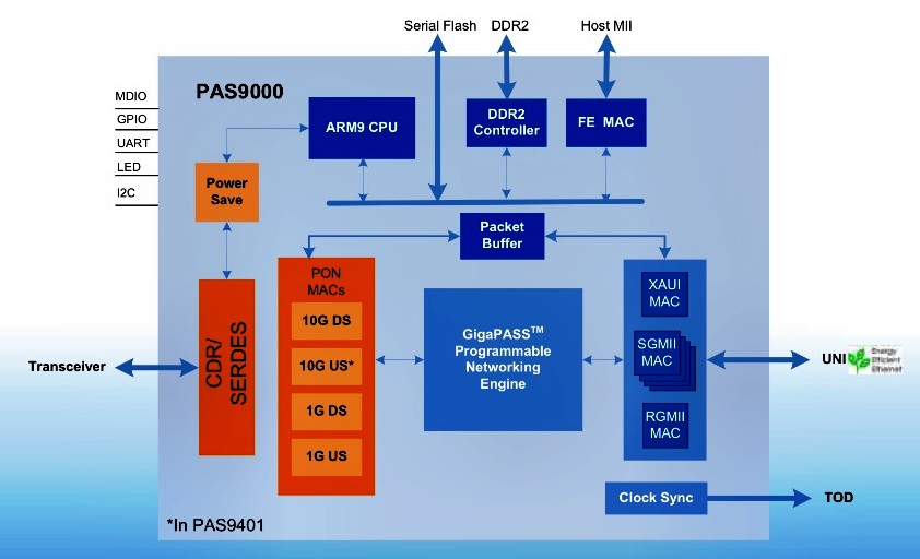 The PAS9000 optical network unit chip architecture. There are two devices in the family. One, the PAS9401, also supports 10G-EPON symmetric mode. Source: PMC-Sierra.
PON Market
PMC-Sierra says that the total market for PON is set for strong growth through 2015.
Using market data from Gartner and IDC, PMC says the 2010 market for EPON silicon was US $120M, growing to $180M for EPON and 10G-EPON speeds in 2015. In contrast, the GPON market was $35M in 2010 but will total $175M for both GPON and XGPON by 2015.
"China is going to be a very large market [for PON] compared to elsewhere," says Rammy Bahalul, senior marketing manager, FTTH division at PMC-Sierra.
Field trials of 10G-EPON have already been conducted in South Korea, Japan and China, says Bahalul: "We see Japan being the first to move to 10G-EPON, followed by Korea and China."
PMC expects 10G-EPON deployments to start in 2013, with the first application being multi-dwelling units. Meanwhile, the company expects first deployments of XGPON in 2014, with field trials starting in 2013. China is expected to deploy XGPON first, followed by North America.
10G-EPON ICs
The 40nm CMOS PAS8000 OLT family comprises four devices.
The PAS8301 and PAS8311 support asymmetric (1Gbps upstream) 10G-EPON. The two chips differ in that the PAS8311 has an on-chip traffic manager/ packet processor which inspects and classifies packets as well as rate-limits particular service flows.
The remaining two devices, the PAS8401 and PAS8411, support symmetric and asymmetric modes. However, the PAS8401 does not include the traffic manager/ packet processor.
All four have the Power Save mode which PMC claims halves the power consumption compared to existing ONUs. For example, it allows the ONU to be shut down when appropriate. The OLT devices also support synchronisation protocols required for mobile backhaul.
Another feature of the PAS8000 family is an on-chip optical time-domain reflectometer (OTDR). The OTDR function enables operators to locate fibre faults without using standalone test equipment, and can diagnose the nature and location of a fault to within a 2m accuracy, says Bahalul.
The PAS9000 ONU family comprises two devices: the asymmetric PAS9301 and the asymmetric/ symmetric PAS9401. The devices support the power save mode and mobile backhaul. And by delivering 10G-EPON symmetric and asymmetric modes, the PAS9401 ONU IC enables operators to plan five years ahead using silicon available now, says Bahalul.
Meanwhile, the company's XGPON OLT and ONU are asymmetric designs - 10Gbps downstream and 2.5Gbps upstream. The system-on-chip XGPON versions have still to be taped out with the designs currently implemented as FPGAs. The XGPON design was part of a recent successful interoperability test, conducted by industry body FSAN (Full Service Access Network), says PMC.
PMC-Sierra says it has a single software development kit that allows software developed on one platform to be reused across all its products.
Altera optical FPGA in 100 Gigabit Ethernet traffic demo
Altera is demonstrating its optical FPGA at OFC/NFOEC, being held in Los Angeles this week. The FPGA, coupled to parallel optical interfaces, is being used to send and receive 100 Gigabit Ethernet packets of various sizes.
The technology demonstrator comprises an Altera Stratix IV FPGA with 28, 11.3Gbps electrical transceivers coupled to two Avago Technologies' MicroPod optical modules.
 "FPGAs are now being used for full system level solutions"
Kevin Cackovic, Altera
The MicroPods - a 12x10Gbps transmitter and a 12x10Gbps optical transceiver - are co-packaged with the FPGA. "All the interconnect between the serdes and the optics are on the package, not on the board," says Steve Sharp, marketing program manager, fiber optic products division at Avago. Such a design benefits signal integrity and power consumption, he says: "It opens up a different world for FPGA users, and for system integration for optic users."
Both Altera and Avago stress that the optical FPGA has been designed deliberately using proven technologies. "We wanted to focus on demonstrating the integration of the optics, not pushing either of the process technologies to the absolute edge," says Sharp.
The nature of FPGA designs has changed in recent years, says Kevin Cackovic, senior strategic marketing manager of Altera's transmission business unit. Many designs no longer use FPGAs solely to interface application-specific standard products to ASICs, or as a co-processor. "FPGAs are now being used for full system level solutions, things like a framer or MAC technology, forward error correction at very high rates, mapper engines, packet processing and traffic management," he says.
Having its FPGAs in such designs has highlighted for Altera current and upcoming system bottlenecks. "This is what is driving our interest in looking at this technology and what is possible integrating the optics into the FPGA," says Cackovic. Applications requiring the higher bandwidth and the greater reach of optical - rack-to-rack rather than chip-to-module - include next-generation video, cloud computing and 3D gaming, he says.
Altera has still to announce its product plans regarding the optical FPGA dsign. Meanwhile Avago says it is looking at higher-speed versions of MicroPod.
"The request for higher line rates is obviously there," says Sharp. "Whether it goes all the way to 28 [Gigabit] or one of the steps in-between, we are not sure yet."
Transport processors now at 100 Gigabit
Cortina Systems has detailed its CS605x family of transport processors that support 100 Gigabit Ethernet and Optical Transport Network (OTN).
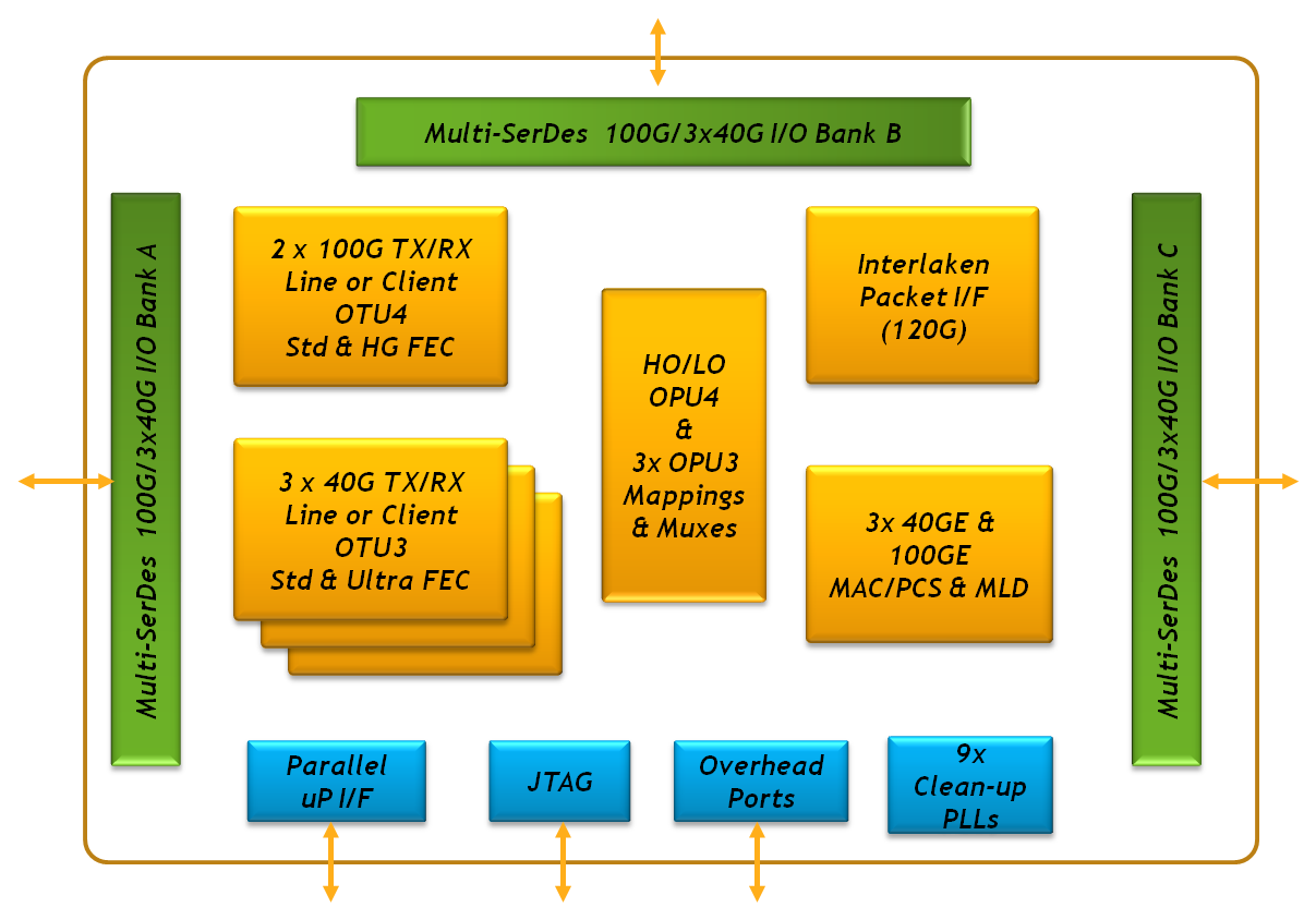 The CS6051 transport processor architecture. Source: Cortina Systems
The application-specific standard product (ASSP) family from Cortina Systems is aimed at dense wavelength division multiplexing (DWDM) platforms, packet optical transport systems, carrier Ethernet switch routers and Internet Protocol edge and core routers. The chip family can also be used in data centre top-of-rack Ethernet aggregation switches.
"Our traditional business in OTN has been in the WDM market," says Alex Afshar, product line manager, transport products at Cortina Systems. "What we see now is demand across all those platforms."
ASSP versus FPGA
Until now, equipment makers have used field programmable gate arrays (FPGAs) to implement 100 Gigabit-per-second (Gbps) designs. This is an important sector for FPGA vendors, with Altera and Xilinx making several company acquisitions to bolster their IP offerings to address the high end sector. System vendors have also used FPGA board-based designs from specialist firm TPACK, acquired by Applied Micro in 2010.
The advantage of an FPGA design is that it allows faster entry to market, while supporting relevant standards as they mature. FPGAs also enable equipment makers to use their proprietary intellectual property (IP); for example, advanced forward error correction (FEC) codes, to distinguish their designs.
However, once a market reaches a certain maturity, ASSPs become available. "ASSPs are more efficient in terms of cost, power and integration," says Afshar.
But industry analysts point out that ASSP vendors have a battle on their hands. "In this class of product, there is a lot of customisation and proprietary design and FPGAs are well suited for that," says Jag Bolaria, senior analyst at The Linley Group.
CS605x family
The CS605x extends Cortina's existing CS604x 40Gbps OTN transport processors launched in April 2011. The CS605x devices aggregate 40 Gigabit Ethernet or OTN streams into 100Gbps or map between 100 Gigabit Ethernet and OTN frames. Combining devices from the two families enables 10 and 40 Gigabit OTN/ Ethernet traffic to be aggregated into 100 Gigabit streams.
The CS6051 is the 100 Gigabit family's flagship device. The CS6051 can interface directly to three 40Gbps optical modules, a 100 Gigabit CFP or a 12x10Gbit/s CXP module. The device also supports the Interlaken interface to 120 Gigabit (10x12.5Gbps) to interface to devices such as network processors, traffic managers and FPGAs.
The CS6051 supports several forward error correction (FEC) codes including the standard G.709, a 9.4dB coding gain FEC with only a 7% overhead, and an 'ultra-FEC' whose strength can be varied with overhead, from 7% to 20%.
The CS6053 is similar to the CS6051 but uses a standard G.709 FEC only, aimed at system vendors with their own powerful FECs such as the latest soft-decision FEC. The CS6052 supports Ethernet and OTN mapping but not aggregation while the CS6054 supports Ethernet only. It is the C6054 which is used for top-of-rack switches in the data centre.
The devices consume between 10-12W. Samples of the CS605x family have been available since October 2011 and will be in volume production in the first half of this year.
Further reading:
For a more detailed discussion of the C605x family, click on the article featured in New Electronics
FPGA transceiver speed hikes bring optics to the fore

Despite rapid increases in the transceiver speeds of field-programmable gate arrays (FPGA), the transition to optical has begun.
FPGA vendors Xilinx and Altera have increased their on-chip transceiver speeds fourfold since 2005, from 6.5Gbps to 28Gbps. But signal integrity issues and the rapid decline in reach associated with higher speed means optics is becoming a relevant option.
Altera has unveiled a prototype with two 12x10Gbps optical engines but has yet to reveal its product plans. Xilinx believes that FPGA optical interfaces are still several years off with requirements being met with electrical interfaces for now.
Altera unveils its optical FPGA prototype
Altera has been showcasing a field-programmable gate array (FPGA) chip with optical interfaces. The 'optical FPGA' prototype makes use of parallel optical interfaces from Avago Technologies.
Combining the FPGA with optics extends the reach of the chip's transceivers to up to 100m. Such a device, once commercially available, will be used to connect high-speed electronics on a line card without requiring exotic printed circuit board (PCB) materials. An optical FPGA will also be used to link equipment such as Ethernet switches in the data centre.
"It is solving a problem the industry is going to face," says Craig Davis, product marketing manager at Altera. "As you go to faster bit-rate transceivers, the losses on the PCB become huge."
What has been done
Altera's optical FPGA technology demonstrator combines a large FPGA - a Stratix IV EP4S100G5 - to two Avago 'MicroPod' 12x10.3 Gigabit-per-second (Gbps) optical engines.
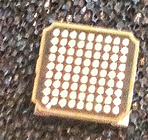 Avago's MicroPod 12x10Gbps optical engine deviceThe FPGA used has 28, 11.3Gbps electrical transceivers and in the optical FPGA implementation, 12 of the interfaces connect to the two MicroPods, a transmitter optical sub-assembly (TOSA) and a receiver optical sub-assembly (ROSA).
The MicroPod measures 8x8mm and uses 850nm VCSELs. The two optical engines interface to a MTP connector and consume 2-3W. Each MicroPod sits in a housing - a land grid array compression socket - that is integrated as part of the FPGA package.
"The reason we are doing it [the demonstrator] with a 10 Gig FPGA and 10 Gig transceivers is that they are known, good technologies," says Davis. "It is a production GT part and known Avago optics."
Why it matters
FPGAs, with their huge digital logic resources and multiple high-speed electrical interfaces, are playing an increasingly important role in telecom and datacom equipment as the cost to develop application-specific standard product (ASSP) devices continues to rise.
The 40nm-CMOS Stratix IV FPGA family have up to 32, 11.3Gbps transceivers, while Altera's latest 28nm Stratix V FPGAs support up to 66x14.1Gbps transceivers, or 4x28Gbps and 32x12.5Gbps electrical transceivers on-chip.
Altera's FPGAs can implement the 10GBASE-KR backplane standard at spans of up to 40 inches. "You have got the distances on the line card, the two end connectors and whatever the distances are across a 19-inch rack," says Davis. Moving to 28Gbps transceivers, the distance is reduced significantly to several inches only. To counter such losses expensive PCBs must be used.
One way to solve this problem is to go optical, says Davis. Adding 12-channel 10Gbps optical engines means that the reach of the FPGAs is up to 100m, simplifying PCB design and reducing cost while enabling racks and systems to be linked.
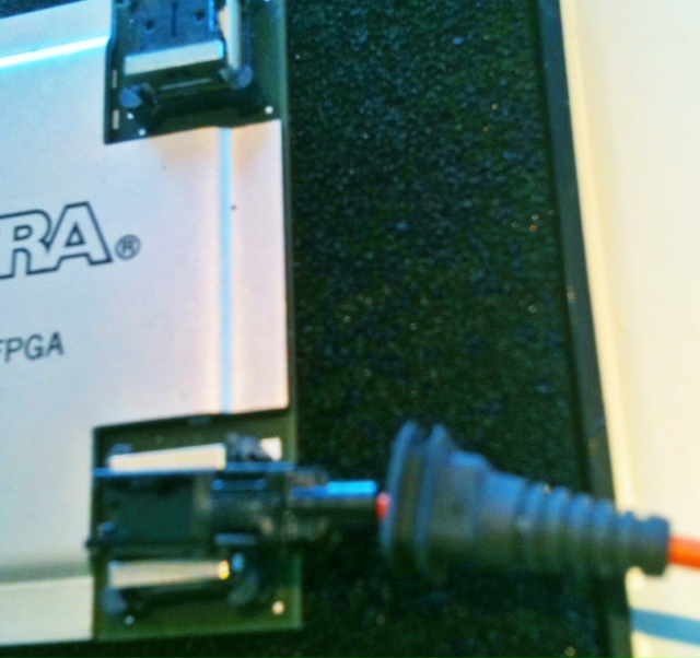 The multimode fibre connector to the MicroPod
Developing an optical FPGA prototype highlights that chip vendors already recognise the role optical interfaces will play.
It is also good news for optical component players as the chip market promises a future with orders of magnitude greater volumes than the traditional telecom market.
The optical FPGA is one target market for silicon photonics players. One, Luxtera, has already demonstrated its technology operating at 28Gbps.
What next
Altera stresses that this is a technology demonstrator only.
The company has not made any announcements regarding when its first optical FPGA product will be launched, and whether the optical technology will enter the market interfacing to its FPGAs' 11.3Gbps, 14.1Gbps or highest-speed 28Gbps transceivers.
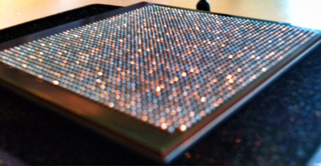 The undersideof the FPGA, showing the 1,932-pin ball grid array
OIF promotes uni-fabric switches & 100G transmitter
 The OIF's OTN implementation agreement (IA) allows a packet fabric to also switch OTN traffic. The result is that operators can now use one switch for both traffic types, aiding IP/ Ethernet and OTN convergence. Source: OIF
Improving the switching capabilities of telecom platforms without redesigning the switch as well as tinier 100 Gigabit transmitters are just two recent initiatives of the Optical Internetworking Forum (OIF).
The OIF, the industry body tackling design issues not addressed by the IEEE and International Telecommunication Union (ITU) standards bodies, has just completed its OTN-over-Packet-Fabric protocol that enables optical transport network (OTN) traffic to be carried over a packet switch. The protocol works by modifying the line cards at the switch's input and output, leaving the switch itself untouched (see diagram above).
In contrast, the OIF is starting a 100 Gigabit-per-second (Gbps) transmitter design project dubbed the integrated dual-polarisation quadrature modulated transmitter assembly (ITXA). The Working Group aims to expand the 100Gbps applications with a transmitter design half the size of the OIF's existing 100Gbps transmitter module.
The Working Group also wants greater involvement from the system vendors to ensure the resulting 100 Gig design is not conservative. "We joke about three types of people that attend these [working group] meetings," says Karl Gass, the OIF’s Physical and Link Layer Working Group vice-chair. "The first group has something they want to get done, the second group has something already and they don't want something to get done, and the third group want to watch." Quite often it is the system vendors that fall into this third group, he says.
OTN-over-Packet-Fabric protocol
The OTN protocol enable a single switch fabric to be used for both traffic types - packets and time-division multiplexed (TDM) OTN - to save cost for the operators.
"OTN is out there while Ethernet is prevalent," says Winston Mok, technical author of the OTN implementation agreement. "What we would like to do is enable boxes to be built that can do both economically."
 The existing arrangement where separate packet and OTN time-division multiplexing (TDM) switches are required. Source: OIF
Platforms using the protocol are coming to market. ECI Telecom says its recently announced Apollo family is one of the first OTN platforms to use the technique.
The protocol works by segmenting OTN traffic into a packet format that is then switched before being reconstructed at the output line card. To do this, the constant bit-rate OTN traffic is chopped up so that it can easily go through the switch as a packet. "We want to keep the [switch] fabric agnostic to this operation," says Mok. "Only the line cards need to do the adaptations."
The OTN traffic also has timing information which the protocol must convey as it passes through the switch. The OIF's solution is to vary the size of the chopped-up OTN packets. The packet is nominally 128-bytes long. But the size will occasionally be varied to 127 and 126 bytes as required. These sequences are interpreted at the output of the switch as rate information and used to control a phase-locked loop.
Mok says the implementation agreement document that describes the protocol is now available. The protocol does not define the physical layer interface connecting the line card to the switch, however. "Most people have their own physical layer," says Mok.
100 Gig ITXA
The ITXA project will add to the OIF's existing integrated transmitter document. The original document addresses the 100 Gigabit transmitter for dual-polarisation, quadrature phase-shift keying (DP-QPSK) for long-haul optical transmission. The OIF has also defined 100Gbps receiver assembly and tunable laser documents.
The latest ITXA Working Group has two goals: to shrink the size of the assembly to lower cost and increase the number of 100Gbps interfaces on a line card, and to expand the applications to include metro. The ITXA will still address 100Gbps coherent designs but will not be confined to DP-QPSK, says Gass.
"We started out with a 7x5-inch module and now there is interest from system vendors and module makers to go to smaller [optical module] form factors," says Gass. "There is also interest from other modulator vendors that want in on the game."
The reduce size, the ITXA will support other modulator technologies besides lithium niobate that is used for long-haul. These include indium phosphide, gallium arsenide and polymer-based modulators.
Gass stresses that the ITXA is not a replacement for the current transmitter implementation. "We are not going to get the 'quality' that we need for long-haul applications out of other modulator technologies," he says. "This is not a Gen II [design].
The Working Group's aim is to determine the 'greatest common denominator' for this component. "We are trying to get the smallest form factor possible that several vendors can agree on," says Gass. "To come out with a common pin out, common control, common RF (radio frequency) interface, things like that."
Gass says the work directions are still open for consideration. For example, adding the laser with the modulator. "We can come up with a higher level of integration if we consider adding the laser, to have a more integrated transmitter module," says Gass.
As for wanting great system-vendor input, the Working Group wants more of their system-requirement insights to avoid the design becoming too restrictive.
"You end up with component vendors that do all the work and they want to be conservative," says Gass. "The component vendors don't want to push the boundaries as they want to hit the widest possible customer base."
Gass expects the ITXA work to take a year, with system demonstrations starting around mid-2013.
How ClariPhy aims to win over the system vendors

“We can build 200 million logic gate designs”
Reza Norouzian, ClariPhy
ClariPhy is in the camp that believes that the 100 Gigabit-per-second (Gbps) market is developing faster than people first thought. “What that means is that instead of it [100Gbps] being deployed in large volumes in 2015, it might be 2014,” says Reza Norouzian, vice president of worldwide sales and business development at ClariPhy.
Yet the fabless chip company is also glad it offers a 40Gbps coherent IC as this market continues to ramp while 100Gbps matures and overcomes hurdles common to new technology: The 100Gbps industry has yet to develop a cost-effective solution or a stable component supply that will scale with demand.
Another challenge facing the industry is reducing the power consumption of 100Gbps systems, says Norouzian. The need to remove the heat from a 100Gbp design - the ASIC and other components - is limiting the equipment port density achievable. “If you require three slots to do 100 Gig - whereas before you could use these slots to do 20 or 30, 10 Gig lines - you are not achieving the density and economies of scale hoped for,” says Norouzian.
40G and 100G coherent ASICs
ClariPhy has chosen a 40nm CMOS process to implement its 40Gbps coherent chip, the CL4010. But it has since decided to adopt 28nm CMOS for its 100Gbps design – the CL10010 - to integrate features such as soft-decision forward error correction (see New Electronics' article on SD-FEC) and reduce the chip’s power dissipation.
The CL4010 integrates analogue-to-digital and digital-to-analogue converters, a digital signal processor (DSP) and a multiplexer/ demultiplexer on-chip. “Normally the mux is a separate chip and we have integrated that,” says Norouzian.
The first CL4010 samples were delivered to select customers three months ago and the company expects volume production to start by the end of September. The CL4010 also interoperates with Cortina Systems’ optical transport network (OTN) processor family of devices, says the company.
The start-up claims there is strong demand for the CL4010. “When we ask them [operators]: ‘With all the hoopla about 100 Gig, why are you buying all this 40 Gig?’, the answer is that it is a pragmatic solution and one they can ship today,” says Norouzian.
ClariPhy expects 40Gbps volumes to continue to ramp for the next three or four years, partly because of the current high power consumption of 100Gbps. The company says several system vendors are using the CL4010 in addition to optical module customers.
The 28nm 100Gbps CL10010 is a 100 million gate ASIC. ClariPhy acknowledges it will not be first to market with an 100Gbps ASIC but that by using the latest CMOS process it will be well position once volume deployments start from 2014.
ClariPhy is already producing a quad-10Gbps chip implementing the maximum likelihood sequence estimation (MLSE) algorithm used for dispersion compensation in enterprise applications. The device covers links up to 80km (10GBASE-ZR) but the main focus is for 10GBASE-LRM (220m+) applications. “Line cards that used to have four times 10Gbps lanes now are moving to 24 and will use six of these chips,” says Norouzian. The device sits on the card and interfaces with SFP+ or Quad-SFP optical modules.
“The CL10010 is the platform to demonstrate all that we can do but some customers [with IP] will get their own derivatives”
System vendor design wins
The 100Gbps transmission ASIC market may be in its infancy but the market is already highly competitive with clear supply lines to the system vendors.
Several leading system vendors have decided to develop their own ASICs. Alcatel-Lucent, Ciena, Cisco Systems (with the acquisition of CoreOptics), Huawei and Infinera all have in-house 100Gbps ASIC designs.
System vendors have justified the high development cost of the ASIC to get a time-to-market advantage rather than wait for 100Gbps optical modules to become available. Norouzian also says such internally-developed 100Gbps line card designs deliver a higher 100Gbps port density when compared to a module-based card.
Alternatively, system vendors can wait for 100Gbps optical modules to become available from the likes of an Oclaro or an Opnext. Such modules may include merchant silicon from the likes of a ClariPhy or may be internally developed, as with Opnext.
System vendors may also buy 100Gbps merchant silicon directly for their own 100Gbps line card designs. Several merchant chip vendors are targeting the coherent marketplace in addition to ClariPhy. These include such players as MultiPhy and PMC-Sierra while other firms are known to be developing silicon.
Given such merchant IC competition and the fact that leading system vendors have in-house designs, is the 100Gbps opportunity already limited for ClariPhy?
Norouzian's response is that the company, unlike its competitors, has already supplied 40Gbps coherent chips, proving the company’s mixed signal and DSP expertise. The CL10010 chip is also the first publicly announced 28nm design, he says: “Our standard product will leapfrog first generation and maybe even second generation [100Gbps] system vendor designs.”
The equipment makers' management will have to decide whether to fund the development of their own second-generation ASICs or consider using ClariPhy’s 28nm design.
ClariPhy acknowledges that leading system vendors have their own core 100Gbps intellectual property (IP) and so offers vendors a design service to develop their own custom systems-on-chip. For example a system vendor could use ClariPhy's design but replace the DSP core with the system vendor’s own hardware block and software.
 Source: ClariPhy Communications
Norouzian says system vendors making 100Gbps ASICs develop their own intellectual property (IP) blocks and algorithms and use companies like IBM or Fujitsu to make the design. ClariPhy offers a similar service while also being able to offer its own 100Gbps IP as required. “The CL10010 is the platform to demonstrate all that we can do,” says Norouzian. “But some customers [with IP] will get their own derivatives.”
The firm has already made such custom coherent devices using customers’ IP but will not say whether these were 40 or 100Gbps designs.
Market view
ClariPhy claims operator interest in 40Gbps coherent is not so much because of its superior reach but its flexibility when deployed in networks alongside existing 10Gbps wavelengths. “You don't have to worry about [dispersion] compensation along routes,” says Norouzian, adding that coherent technology simplifies deployments in the metro as well as regional links.
And while ClariPhy’s focus is on coherent systems, the company agrees with other 100Gbps chip specialists such as MultiPhy for the need for 100Gbps direct-detect solutions for distances beyond 40km. “It is very likely that we will do something like that if the market demand was there,” says Norouzian. But for now ClariPhy views mid-range 100Gbps applications as a niche opportunity.
Funding
ClariPhy raised US $14 million in June. The biggest investor in this latest round was Nokia Siemens Networks (NSN).
An NSN spokesperson says working with ClariPhy will help the system vendor develop technology beyond 100Gbps. “It also gives us a clear competitive edge in the optical network markets, because ClariPhy’s coherent IC and technology portfolio will enable us to offer differentiated and scalable products,” says the spokesperson.
The funding follows a previous round of $24 million in May 2010 where the investors included Oclaro. ClariPhy has a long working relationship with the optical components company that started with Bookham, which formed Oclaro after it merged with Avanex.
“At 100Gbps, Oclaro get some amount of exclusivity as a module supplier but there is another module supplier that also gets access to this solution,” says Norouzian. This second module supplier has worked with ClariPhy in developing the design.
ClariPhy will also supply the CL10010 to the system vendors. “There are no limitations for us to work with OEMs,” he says.
The latest investment will be used to fund the company's R&D effort in 100, 200 and 400Gbps, and getting the CL4010 to production.
Beyond 100 Gig
The challenge at higher data rates that 100Gbps is implementing ultra-large ASICs: closing the timings and laying out vast digital circuitry. This is an area the company has been investing in over the last 18 months. “Now we can build 200 million logic gate designs,” says Norouzian.
Moving from 100Gbps to 200Gbps wavelengths will require higher order modulation, says Norouzian, and this is within the realm of its ASIC.
Going to 400Gbps will require using two devices in parallel. One Terabit transmission however will be far harder. “Going to one Terabit requires a whole new decade of development,” he says.
Further reading:
Network processors to support multiple 100 Gigabit flows

“We don’t know of any device, announced at least, that comes close to this”
Amir Eyal, EZchip
The NP-5 is noteworthy in integrating within a single chip a full-duplex 100 Gigabit-per-second (Gbps) packet processor and traffic manager. Such integration is important as line cards move from 100Gbps to 400Gbps densities, says Bob Wheeler, senior analyst at The Linley Group.
Target markets
The NP-5 is aimed at router and transport switches platforms that make up the carrier Ethernet switch router (CESR) market. Platforms include packet optical transport switches and edge routers. Infonetics Research forecasts that the total Carrier Ethernet market will grow to US $37bn in 2015 from $26bn in 2010, while the CESR market will double to $20bn by 2015.
EZchip says its main competition is in-house ASIC design teams of the large system vendors. Alcatel-Lucent for example has just announced its FP3 400Gbps network processor. The FP3 is implemented as a three-device chipset made up of a packet processor, traffic manager and a fabric-access chip.
EZchip also believes the device has a role within the data centre. New protocol developments require packet processing that today can only be achieved using a packet processor, it says.
An example is OpenFlow which EZchip supports using its current NP-4 processor. OpenFlow is an academic initiative that allows networking protocols to be explored on existing switch hardware but it is of growing interest to data centre operators. The initiative creates an industry-standard application programming interface (API) to the underlying switch platforms.
The latest OpenFlow version (V1.1) can only be supported using a network processor, says Amir Eyal, EZChip’s vice president of business development. However the data centre is seen as a secondary market for the NP-5. The downside is that the NP-5 and similar network processors targeted at telecoms cost more than switch ASICs from vendors. Only when the functionality of an NPU is needed will vendors pay more.
NP-5 architecture
The chip's main functional blocks are a programmable packet processor and a traffic manager. Also integrated on-chip is an integrated Ethernet switch fabric adaptor, media access controllers (MACs) that support 1, 10, 40 and 100 Gigabit Ethernet (GbE), and a memory controller designed for use with DDR3 external memory to reduce overall system cost. The current NP-4 supports DDR3 and RLDRAM - considerably more expensive than DDR3.
The packet processing is performed using task-optimised processor engines (TOPs). Four styles of TOP engines are used: Two perform classification - parsing, which extracts packet headers and data fields, and searching using look-up tables; and one TOP each for packet modification and packet forwarding.
Each TOP has a 64-bit architecture and processes a single thread. A scheduler allocates a packet to the next available free TOP. EZchip does not disclose the number of TOPs it uses but says that the NP-5 will have almost twice the number used for the NP-4, with the most numerous being the search TOP due to the numerous look-ups needed.
An on-chip ternary content addressable memory (TCAM), meanwhile, supports more sophisticated look-ups and operates in parallel to the simpler TOPs-based searches.
The traffic manager provides bandwidth and guarantees a certain service level performance to particular packet flows. The traffic manager makes decisions when packet congestion occurs based on a given traffic’s priority and its associated rules.
The NP-5 first stores packets in its internal buffer memory before dropping lower-priority packets once memory is full. It is rare that all the input ports are full simultaneously. By taking advantage of the integrated MACs on-chip, up to 24, 10 Gigabit ports can be used to input data. The NP-5 can thus support peak flows of 240Gbps, or a 2.4-to-1 oversubscription rate, equating to a system line card supporting 24-ports at 10Gbps traffic at the same cost as a 10 port-10Gbps design, says EZchip.
The NP-5 will also have four integrated engines. Each engine will support either 12x10GbE, 3x40GbE, 1x100GbE or one Interlaken interface. Two of the four interface engines support 48, 1GbE ports using the QSGMII interface while the remaining two support 12x1GbE ports using the SFI interface.
The QSGMII interface allows a quadrupling of the links by interleaving four ports per link. However an additional external device is needed to break the four interleaved ports into four separate ones. The SFI interface allows a direct connection to a 1GbE optical module.
Also included on the device is an Ethernet fabric adapter that supports 24, 10Gbps (10GBASE-KR) short-reach backplane interfaces.
Device metrics
The 200Gbps NP-5 will be able to process up to 300 million 64byte packets per second. The chip’s power consumption is estimated at 50W. Implemented using a 28nm CMOS process, the device will require 2,401 pins.
What next?
The NP-5 is scheduled to sample year-end 2012. Assuming it takes 18 months to design systems, it will be mid-2014 when NP-5 line cards supporting multiple 100Gbps interfaces are first deployed. EZchip says four or even eight NP-5s could be integrated on a line card, achieving a total packet throughput of 1.6Tbit/s per board.
Meanwhile EZchip’s NP-4 is currently sampling and will ramp in the next few months. Most of the large edge router and switch vendors are designing the NP-4 into their systems, says EZchip.
Further reading:
For more NP-5 detail see the New Electronics article, click here.
