
Timepieces that tell you how you are
Apple is Rockley Photonics’ largest customer. So says Rockley in a document filed with the US Securities and Exchange Commission (SEC) as it prepares to be listed on the New York Stock Exchange (NYSE).
The Form S-4 document provides details of Rockley’s silicon photonics platform for consumer ‘wearables’ and medical devices, part of the emerging health and wellness market.
Andrew Rickman, Rockley Photonics’s CEO, discusses what the company has been working on and how a wearable device can determine a user’s health.
The first of several articles on silicon photonics-based biosensors for medical and other applications.
Andrew Rickman
Part 1: Consumer Wearables
Ever wondered what the shining green light is doing on the underside of your smartwatch?
The green LED probes the skin to measure various health parameters - biomarkers - of the wearer. Just what light can reveal about a user’s health is a topic that has preoccupied Rockley Photonics for several years.
Rockley is not solely interested in using the visible spectrum to probe the skin but also light at higher wavelengths. Using the infrared portion of the spectrum promises to reveal more about the watch wearer's health.
Rockley can also shed light on its own healthcare activities following the announcement of its merger with SC Health that will enable Rockley to be listed on the NYSE, valued at $1.2 billion.
SC Health is a Special Purpose Acquisitions Company or SPAC. Also known as a ‘blank cheque’ company, a SPAC is a publicly listed cash shell company that raises money to acquire an early-stage start-up before its listing.
For Andrew Rickman, who will remain as Rockley’s CEO, the latest development is consistent with his silicon photonics vision when he established Bookham Technologies in 1988.
He views silicon photonics as an enabling technology, a platform that can address multiple industries, the healthcare market being the most promising. As such, Rockley is no more a healthcare company than it is an optical transceiver or a LiDAR player, says Rickman.
SPAC path
Rockley is not commenting on the SC Health transaction except to say that start-ups aspire to go public or be acquired. “We are going public through this route,” says Rickman.
The company can’t say much about SC Health either. What Rickman will say is that shell companies are created by people with a particular industry background: “Clearly, there is a very big health dimension to Rockley, and SC Health is a health-oriented SPAC.”
Rockley’s silicon photonics platform is already being used for the optical transceiver market through a joint venture with Hengtong Optic-Electric. Rockley is also working with partners to develop co-packaged optics solutions, where its optics is packaged alongside a chip to enable optical input-output.
The company’s other interests include advanced optical computing, environmental sensing, vision systems/ LiDAR and spectroscopy, its approach for wearable and medical diagnostics devices.
The medical diagnostics market uses ‘invasive’ techniques where lab equipment analyses samples such as blood, saliva and urine. In contrast, the non-invasive health market was largely created with the advent of smartwatches, says Rickman. Here the light is used to probe under the skin where it is scattered. The reflected light is then analysed by the watch.
Rickman says that, unlike the established medical diagnostics market, knowledge and expertise for the newer non-invasive approach is limited: “It creates an opportunity for us to fill the gap.”
Rockley’s expertise ranges from the semiconductor process needed to make the sensor and the measurement and analysis of the data collected.
Medical diagnostics
Medical diagnostic equipment analysing a blood sample, for example, determines its many constituents. Specially designed biochemical ‘labels’ are used that attach to what is being detected. Such labels are fluorescent so that the degree of binding and hence the amount of tested-for material is determined by measuring the degree of fluorescence, says Rickman.
Silicon photonics start-ups are among firms developing alternative equipment that is “label-free” and does not require fluorescent labels. Such equipment still requires biochemistry for ‘receptors’ that trap the constituents being tested for. But here what is measured is refractive index changes of the light.
Label-free sensors use silicon photonics circuits that measure the refractive index. The circuits can be a waveguide and ring resonator or a Mach-Zehnder interferometer. Light shined through the circuit undergoes tiny changes in its refractive index caused by constituent-receptor bindings on the sensor’s surface. The circuits are tiny, meaning sensors can be integrated on-chip to measure multiple biomarkers.
Silicon photonics-based biosensors promise more compact diagnostic systems than those used in labs and hospitals. Such systems could be used in ambulances, intensive care units and at a doctor’s office. They can also deliver test results in 25 minutes or less, far quicker than sending samples to a lab and having to wait hours or a day for results.
“There are a lot of companies in this [biosesnor diagnostics] field,” says Rickman. “It is a field deserving close attention and is an exciting area.” However, Rockley’s focus is non-invasive wearables instead.
Wearables cannot match the diagnostic detail provided by invasive techniques, says Rickman. But non-invasive techniques have much scope for diagnostic improvement compared to existing smartwatches.
And while a blood test may provide far greater detail, it indicates only what is happening when a sample is taken. A wearable, in contrast, can continuously monitor the user. This creates new healthcare opportunities, say Rickman.
LEDs and lasers
The technique underpinning smartwatch monitoring has the long title of non-invasive diffuse reflective spectroscopy.
Light at different wavelengths penetrates the skin and is scattered by blood vessels and cells and the interstitial fluid in between. The reflected light is analysed using spectroscopy to glean medical insights.
The smartwatch uses a green LED since blood haemoglobin has a good light absorption at that wavelength. “Effectively, what is being measured is the expansion and contraction of the blood vessels,” says Rickman. “It is measuring the amount of light that is absorbed by the change of the volume of blood.”
It doesn’t stop there. Using a red LED and extending it into the infrared range, the blood oxygenation level is measured using the ratio of oxygenated (bright red) and unoxygenated (darker red) haemoglobin. “The ratio of the two wavelengths that you get back is proportional to the blood oxygen level,” says Rickman.
The visible range can also detect bilirubin, a yellow-orange bile pigment associated with jaundice.
“But that is pretty much it,” says Rickman. “All the other thousands of constituents, if they have absorption peaks, are swamped in the visual range by haemoglobin.”
What Rockley has done is extend the light’s spectral to measure absorption peaks that otherwise are dwarfed by water and haemoglobin.
“We are addressing the visible range and extending it into the infrared range, getting much more accuracy using laser technology compared to LEDs which opens up a whole range of things,” says Rickman.

To do this, Rockley has used its silicon photonics expertise to shrink a benchtop spectrometer to the size of a chip. Normally miniaturisation reduces performance. For a start, the size of the aperture that collects light is reduced, says Rickman. But Rockley claims its silicon photonics platform and its design improves greatly the signal-to-noise ratio compared to a benchtop spectrometer.
“We are talking orders of magnitude improvement over the best-in-class benchtop instruments,” says Rickman.
An important parameter associated with optical transceivers is the link budget, says Rockley, which means getting enough signal to the receiver to recover the data sent. This is defined as part of a standard and being compliant requires meeting the specification.
“Here [with spectroscopy], no one is determining the performance that must be met; there is no standard,” says Rickman, making it an area ripe for innovation.
Platform process
What a wearable spectrometer must deliver is a highly accurate wavelength registration and a deconvolving of what the spectrum comprises, says Rickman
Rockley says one aspect of its silicon photonics process is its use of relatively large waveguides: several microns wide compared to hundreds of nanometers.
It makes sense for companies to adapt CMOS processes for silicon photonics to create sub-micron waveguides, he says, but if the dimensions are smaller than the light’s wavelength, it becomes highly sensitive to the manufacturing process and polarisation while experiencing higher optical loss.
“With the larger waveguides, we get 20x better wavelength registration,” says Rickman. “That is the difference between being able to make the product, or not.”
Healthcare benefits
Rockley says its spectrometer-on-a-chip measures a range of biophysical and biochemical biomarkers. “It will go a lot further than watches today, a lot deeper but not as deep as a blood draw,” says Rickman.
The sensor can detect lactate, urea, glucose - ‘a tough one but a big one’ - and chemical biomarkers that are in a high proportion in blood, says Rickman
“The diseases that are predominant over life, each one has a handful of biomarkers,” says Rickman. “A non-invasive smartwatch can measure these, providing good indicators of the early onset of a disease.”
Detecting the onset of disease will enable more effective treatment, better patient outcomes and less costly healthcare. “The smartwatch doesn’t have to be conclusive,” says Rickman. It is not replacing a full analysis but it can be an early warning and lead to a better outcome.
Such continuous noninvasive monitoring will also help patients with chronic diseases, improving their treatment.
Rickman didn’t detail what probing with infrared light will enable but the filed S-4 Form says Rockley is exploring the early detection of key diseases. These include coronary arterial disease, diabetes, chronic kidney disease, Covid-19, asthma, hepatitis C, cirrhosis, Alzheimer’s, stroke, flu, sepsis and cancer.
Rickman says there is research looking at detecting early onset Covid-19 using a patient’s vital signs but this requires their presence at a clinic. The parameters monitored include blood sugar, blood pressure, hydration, blood oxygen level and heart rate.
Using the parameters combined with machine learning can determine if a patient will have a bad covid-19 experience or not. If the former, drastic treatment steps can be taken before the patient becomes ill.
Market opportunity
Rickman is excited at the scale of the wearable opportunity. In microelectronics, it is consumer applications that drive economies of scale. There may be millions of units of optical transceivers, he says, but that doesn't achieve ‘hyper-scale. “You want to be making tens of millions of units a week,” he says.
The press release announcing the stock market float referred to Rockley working with world-class partners. Asked about Apple and Samsung, leading makers of smartwatches, Rickman would only say that Rockley is targeting the wearable and medical device markets for customers.
However, the S-4 Form names Apple and other firms such as smartwatch maker Zepp Health, LifeSignals Group which makes wearable medical biosensors, and Withings France SA that makes watches and other healthcare devices. Meanwhile, healthcare company, Medtronic, is a strategic investor in Rockley.
Rockley is projecting revenues of $1.1 billion in 2024 if all goes to plan.
Career passion
Rickman has been interested in silicon photonics and sensing “since the beginning of time”.
He points out how, in the mid-80s, before he founded Bookham, Professor Richard Soref, a silicon photonics luminary, had provided a guide as to what could be done in silicon photonics. “I went on and had the privilege of working with Soref,” says Rickman.
When Rickman investigated the application areas for silicon photonics, he thought that Bell Labs had already solved the problems associated with optical communications so he focussed on sensors. Back then, it was tough to create a multidisciplinary team needed to exploit the biosensor opportunity.
Then, in the late 90s, the dotcom era started and it was clear that many problems remained in making optical-fibre componentry. Bookham dropped its sensor work and focussed exclusively on optical communications.
Rockley was formed in 2013 as a silicon photonics platform company. “It was a question of which of these applications, out of a massive menu that we collected over time, were going to take off in the timeframe of Rockley Photonics,” he says.
Apple watchers have already started speculating as to the features of the next Apple Watch, the Series 7, expected this autumn. In February, one site said the watch is still a long way off and there was little solid news.
The Series 7 watch’s features may be unknown but the direction smartwatches are taking is now much clearer.

Is traffic aggregation the next role for coherent?
Ciena and Infinera have each demonstrated the transmission of 800-gigabit wavelengths over near-1,000km distances, continuing coherent's marked progress. But what next for coherent now that high-end optical transmission is approaching the theoretical limit? Can coherent compete over shorter spans and will it find new uses?
Part 1: XR Optics
“I’m going to be a bit of a historian here,” says Dave Welch, when asked about the future of coherent.
Interest in coherent started with the idea of using electronics rather than optics to tackle dispersion in fibre. Using electronics for dispersion compensation made optical link engineering simpler.

Dave Welch
Coherent then evolved as a way to improve spectral efficiency and reduce the cost of sending traffic, measured in gigabit-per-dollar.
“By moving up the QAM (quadrature amplitude modulation) scale, you got both these benefits,” says Welch, the chief innovation officer at Infinera.
Improving the economics of traffic transmission still drives coherent. Coherent transmission offers predictable performance over a range of distances while non-coherent optics links have limited spans.
But coherent comes at a cost. The receiver needs a local oscillator - a laser source - and a coherent digital signal processor (DSP).
Infinera believes coherent is now entering a phase that will add value to networking. “This is less about coherent and more about the processor that sits within that DSP,” says Welch.
Aggregation
Infinera is developing technology - dubbed XR Optics - that uses coherent for traffic aggregate in the optical domain.
The 'XR’ label is a play on 400ZR, the 400-gigabit pluggable optics coherent standard. XR will enable point-to-point spans like ZR optics but also point-to-multipoint links.
Infinera, working with network operators, has been assessing XR optics’ role in the network. The studies highlight how traffic aggregation dictates networking costs.
“If you aggregate traffic in the optical realm and avoid going through a digital conversion to aggregate information, your network costs plummet,” says Welch.
Are there network developments that are ripe for such optical aggregation?
“The expansion of bandwidth demand at the network edge,” says Rob Shore, Infinera’s senior vice president of marketing. “It is growing, and it is growing unpredictably.”
XR Optics
XR optics uses coherent technology and Nyquist sub-carriers. Instead of a laser generating a single carrier, pulse-shaping at the optical transmitter is used to create multiple carriers, dubbed Nyquist sub-carriers.
The sub-carriers carry the same information as a single carrier but each one has a lower symbol rate. The lower symbol rate improves tolerance to non-linear fibre effects and enables the use of lower-speed electronics. This benefits long-distance transmissions.
But sub-carriers also enable traffic aggregation. Traffic is fanned out over the Nyquist sub-carriers. This enables modules with different capacities to communicate, using the sub-carrier as a basic data rate. For example, a 25-gigabit single sub-carrier XR module and a 100-gigabit XR module based on four sub-carriers can talk to a 400-gigabit module that supports 16.
It means that optics is no longer limited to a fixed point-to-point link but can support point-to-multipoint links where capacities can be changed adaptively.
“You are not using coherent to improve performance but to increase flexibility and allow dynamic reconfigurability,” says Shore.

Rob Shore
XR optics makes an intermediate-stage aggregation switch redundant since the higher-capacity XR coherent module aggregates the traffic from the lower-capacity edge modules.
The result is a 70 per cent reduction in networking costs: the transceiver count is halved and platforms can be removed from the network.
XR Optics starts to make economic sense at 10-gigabit data rates, says Shore. “It depends on the rest of the architecture and how much of it you can drive out,” he says. “For 25-gigabit data rates, it becomes a virtual no-brainer.”
There may be the coherent ‘tax’ associated with XR Optics but it removes so much networking cost that it proves itself much earlier than a 400ZR module, says Shore.
Applications
First uses of XR Optics will include 5G and distributed access architecture (DAA) whereby cable operators bring fibre closer to the network edge.
XR Optics will likely be adopted in two phases. The first is traditional point-to-point links, just as with 400ZR pluggables.
“For mobile backhaul, what is fascinating is that XR Optics dramatically reduces the expense of your router upgrade cost,” says Welch. “With the ZR model I have to upgrade every router on that ring; in XR I only have to upgrade the routers needing more bandwidth.”
Phase two will be for point-to-multipoint aggregation networks: 5G, followed by cable operators as they expand their fibre footprint.
Aggregation also takes place in the data centre, has coherent a role there?
“The intra-data centre application [of XR Optics] is intriguing in how much you can change in that environment but it is far from proven,” says Welch.
Coherent for point-to-point links will not be used inside the data centre as it doesn’t add value but configurable point-to-multiple links do have merit.
“It is less about coherent and more about the management of how content is sent to various locations in a point-to-multiple or multipoint-to-multipoint way,” says Welch. “That is where the game can be had.”
Uptake
Infinera is working with leading mobile operators regarding using XR Optics for optical aggregation. Infinera is talking to their network architects and technologists at this stage, says Shore.
Given how bandwidth at the network edge is set to expand, operators are keen to explore approaches that promise cost savings. “The people that build mobile networks or cable have told us they need help,” says Shore.
Infinera is developing the coherent DSPs for XR Optics and has teamed with optical module makers Lumentum and II-VI. Other unnamed partners have also joined Infinera to bring the technology to market.
The company will detail its pluggable module strategy including XR Optics and ZR+ later this year.

Silicon photonics' second wave
Two concentric circles drawn in chalk are shown on-screen. So Professor Roel Baets open his plenary talk at the European Conference on Integrated Optics (ECIO) 2020, asking the online audience what is being shown.

Professor Roel Baets
Suggestions come flooding in: the cross-section of an optical fibre, a silicon wafer, a ring resonator optical component and - the correct answer - a doughnut.
The image is from the front cover of Doughnut Economics: Seven Ways to Think Like a 21st-Century Economist by Kate Raworth, a UK professor of economics.
The author discusses how continual economic growth is out of kilter with the planet’s well-being and details alternative approaches. The “doughnut” represents a sweet-spot region ensuring sustainable growth.
Baets applied the book’s thinking to his plenary talk on the topic of silicon photonics research.
Research perspective
Baets’ research work focusses on the use of silicon photonics for applications other than telecom and datacom.
High-speed transceivers for telecom and datacom continue to drive silicon photonics, creating mature platforms and funding the technology’s development.
The two industries will also continue to drive silicon photonics for the coming decade but the picture is set to change. “There is huge potential for other markets; sensing, life sciences and medical being some of them,” he says.
Baets is director of the multidisciplinary Centre for Nano- and Biophotonics at Ghent University in Belgium. His research group comprises 90 staff, split between Ghent University and imec, the renowned R&D centre. “We are sort of a hybrid unit, part university and part imec,” he says.
His focus on the next wave of silicon photonics is partly due to a long-standing interest in biomedical engineering and because high-speed transceiver research is now mainstream.
“I have a big appetite to do something less evolutionary and more groundbreaking,” he says.
Applying the technology to do something helpful appeals to him: “Diagnosing diseases or for therapy of diseases, I feel that is more relevant.”
Background
Baets received the 2020 John Tyndall Award from The Optical Society (OSA) and the IEEE Photonics Society. The award is for his “seminal research in silicon photonics and for driving the foundry model in this field.”
Baets read electrical engineering at Ghent University where he also earned a masters degree. He gained a second masters at Stanford University in California.
“It sounds redundant but I had the privilege of doing a lot of things in terms of subjects that I hadn’t been able to do at Ghent so it was wonderful,” says Baets.
It was at Stanford that Baets pursued his interest in biomedical engineering. He also ‘fell in love’ with photonics after he met and worked with Joseph Goodman, whom he describes as the father of Fourier optics and statistical optics.
That set the course of his photonics research, while his interest in biomedical engineering remained. “And it [biomedical engineering] has popped up in recent years in combination with photonics,” he says.
Foundry model
Baets compares the progress of silicon photonics with that of the chip industry several decades ago.
In the 1970s, universities undertaking integrated circuit research had clean rooms but the growing sophistication of chip-making meant it became too costly.
“Universities and research groups had to give up having their own fabrication facilities for research,” he says.
The same happened within the chip industry, with few chip firms able to afford clean rooms resulting in the advent of foundries.
Even the semiconductor titan Intel, which built its fortune by leading the chip industry in CMOS process technology, is now considering foundries to make its chips.
A similar model is now playing out with integrated photonics.
>
“I believe the field of silicon photonics is at a pivotal point of change and acceleration.”
“The microelectronics fab is an extremely expensive infrastructure,” says Baets. “Maintaining the process flow for certain platforms that enable you to combine [optical] functions on-chip takes quite a bit of diligence and therefore cost.”
This is why creating ‘open’ mechanisms whereby interested parties can gain access to such technology is so important.
“Even if you don’t have a fab in your backyard, there are places you can go to,” says Baets. “That was the essence behind starting ePIXfab.”
Baets helped found ePIXfab, the first global multi-project wafer service for silicon photonics, in 2006.
The idea of multi-project wafers is to aggregate photonic designs from many different users into one mask set before passing a wafer run through a fab. “Multi-project wafers is a cost-sharing process that is well established in electronics,” he says.
Platforms
The Kate Raworth book on sustainable growth was an eye-opener to many people, says Baets, given the topic was addressed by an economist rather than a climate-change scientist.
“Growth is important but there are other dimensions, and you need to find a sweet spot,” he says. “I couldn’t resist using this for my ECIO talk as a metaphor for the field of silicon photonics.”
Silicon photonics is at a turning point, he says, and it will be interesting to see how the field develops over the next five to ten years in terms of finding a way to create mature platforms serving different applications and markets.
The term platform refers to the entire chain of processes that happen in a microelectronics fab, starting with plain wafers and ending with diced chips.
When Baets talks about mature platforms he is referring to a standardised process flow where the basic components are well defined and where a user has some freedom in how the optical functions are connected. It should also be “open access”, similar to CMOS chip foundries.
The technology used for chip-making - the wafer-level processes and the infrastructure - is hugely expensive yet what it produces - the chips - are ‘insanely cheap’, says Baets
“Because of these special boundary conditions, you have to be careful in the research directions you choose,” he says. ”It doesn’t make sense to embark in a direction where it is hard to imagine how it would fit into a sustainable platform.“
This is the essence of his plenary talk.
For example, several places around the world have created a process flow that combines silicon nitride optical waveguides with standard silicon ones. This has only happened in the last couple of years.
“It is a beautiful example of how you can extend the richness of a platform to another level, thereby serving many new applications and customers,” he says.
Meanwhile, a current focus of academic research concerns ways to add III-V lasers to the silica substrate, what he describes as the Holy Grail of silicon photonics.
Baets stresses that there is huge potential for many different applications in the coming years but that it will only happen if real-world products can be made in places that have mature, open-access platforms.
“This is not entirely trivial as it is expensive to establish such platforms,” he says.
There is also this dream of creating a unified platform that can do everything. But Baets says such a generic platform is unrealistic given the overall range of wavelengths used, for datacom, telecom and the longer wavelengths of infra-red.
“You cannot expect one platform to serve all of these,” says Baets. ”But, equally, if there is too much fragmentation, things will not turn out well,” he says.
Baets is aware of at least 20-30 start-up companies developing silicon photonics products, not for datacom or telecom.
In his plenary talk he listed such applications as neuromorphic computing, quantum computing, virtual reality – augmented reality, environmental sensing such as for gas using mid-infrared, critical infrastructure monitoring, and a variery of medical applications such as biosensors, cardiovascular monitoring, glucose monitoring neurophotonics and optical coherence tomography.
Not all these players will be successful but he does expect silicon photonics chips to be made in volumes that will eclipse telecom and datacom in the next five years or so.
But that brings us back to the issue of platforms. “Can they [designers] do things with the existing platforms or do they need a platform that goes a step further - or three steps further?” he says. “And then that question of a unified platform comes up again.”
Training
Baets is dedicating part of his time to address the issue of training in silicon photonics.
“There is a shortage of people with the skills to do silicon photonics,” he says.
Silicon foundries are full of people that understand electronics devices and there is a need for people that understand photonic devices, which are different.
People are also needed with application skills.
“If you think of medical devices, there is a vast distance between expertise in medical-device companies and expertise in the field of silicon photonics,” says Baets. “So there is a need for a lot of bridging work to make people aware of the potential of photonics in general and silicon photonics in particular.”
This is a role ePIXfab has embraced with training activities to address this need.
Research goals
What would Baets like to witness given another decade of uninterrupted research work?
“It is all about impact,” he says. “You would want to see research work turned into something that, at the end of the day, helps people.”
He has great respect for curiosity-driven research. “Curiosity-driven research is like art,” he says. “It is something that is beautiful if done by people with the right skills and is something that society can afford.”
But he is less attracted to conceptual beauty and more to things that prove helpful: “This whole field is about things that help people, whether that is the internet or a medical device.”
Meanwhile, there is COVID-19 to contend with.
As we complete the interview, Baets has a follow-on online meeting with his students.
And the previous evening he attended his first live concert since the start of the COVID-19 lockdown, given by Belgium jazz pianist, Jef Neve. “It was a privilege and it was very enjoyable,” he says.
Classical music is a passion of Baets and in his youth, he played the piano.
“The number of times I now touch the piano is limited but I have some ambition to take it up again,” he says.
Further Information:
Kim Roberts, 2019 John Tyndall Award winner, click here

Silicon Photonics spills over into new markets
The market for silicon photonics is set to grow eightfold by 2025. So claims market research firm, Yole Développement, in its latest report on silicon photonics, a technology that enables optical components to be made on a silicon substrate.
Silicon photonics is also being used in new markets although optical transceivers will still account for the bulk of the revenues in 2025.
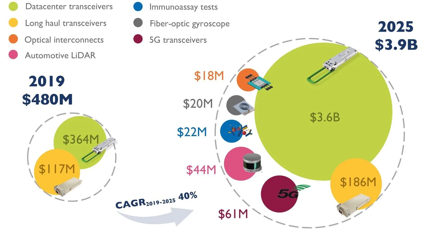
Source: Yole
Market forecast
“We are entering a phase where we are beyond the tipping point [for silicon photonics],” says Eric Mounier, fellow analyst at Yole. “There is no doubt silicon photonics will grow and will be used beyond the data centre.”
Yole sized the 2019 global silicon photonics market at US $480 million, dominated by sales of optical transceivers for the data centre. In 2025 the forecast is for a $3.9 billion market, with data centre transceivers accounting for over 90 per cent of the market.
Eric Mounier
Revenues from new markets such as 5G optical transceivers, automotive, co-packaged optics, fibre-optic gyroscopes, and biochemical sensors will generate $165 million revenues in 2025.
The Yole report also highlights a maturing supply chain, advances in co-packaged optics, and more silicon photonics start-up announcements in the last year.
“It seems the big data centre operators, telecom players and sensor companies are convinced silicon photonics is a key technology for integration, lower cost and smaller components for interconnect and sensing applications,” says Mounier.
Optical transceivers
Data centre optical transceivers account for the bulk of silicon photonics’ market value and unit volumes.
Three-quarters of revenues in 2019 were for data centre transceivers for reaches ranging from several hundred meters to 2km and 10km. This market for silicon photonics is dominated by two players: Intel and Cisco with its Luxtera acquisition.
“For 100-gigabit transceivers, silicon photonics is probably the most used technology compared to legacy optics,” says Mounier.
The remaining 2019 revenues were from long-haul coherent transceiver sales, a market dominated by Acacia that is being acquired by Cisco.
Other companies involved in the transceiver supply chain include Innolight, Juniper Networks, and Alibaba with its work with Elenion Technologies (Elenion was recently acquired by Nokia). HP is working with several firms to develop its silicon photonics supply chain, from device design to final products.
The rollout of 5G is generating a need for 10-gigabit and 25-gigabit transceivers for distances up to 100m, linking remote radio heads and the baseband unit, part of the 5G radio access network.
Yole forecasts a $61 million 5G transceiver market in 2025.
Co-packaged optics
The packaging of optical input-output with a digital chip, known as co-packaged optics, has made notable progress in the last year.
“We are pretty convinced that co-packaged optics is the next big application for silicon photonics,” says Mounier.
Intel has demonstrated its optics packaged with the Tofino 2 Ethernet switch chip it gained with the Barefoot Networks acquisition. “Talking to Intel, I believe in two to three years from now, there will be the first product,” he says.
Other firms pursuing co-packaged optics include Ranovus, Rockley Photonics, Ayar Labs and Sicoya.
The doubling in Ethernet switch-chip capacity every two years is a key driver for co-packaged optics. Switch chips with 25.6-terabit capacity exist and 51.2-terabit switches will be shipping by 2025.
There will also be eight-hundred-gigabit pluggable transceivers in 2025 but Yole says co-packaged optics offers a systems approach to increasing channel counts to keep pace with growing switch capacities.
Foundries and design houses
More than 10 foundries exist worldwide offering silicon photonics services.
“Foundries are interested in silicon photonics because they see a future opportunity for them to fill their fabs,” says Mounier.
Yole cites how GlobalFoundries is working with Ayar Labs, HP with TSMC, Sicoya with IHP Microelectronics, and Rockley Photonics with VTT Memsfab. TSMC also works with Cisco through its Luxtera acquisition.
Swedish MEMS foundry, Silex Microsystems, is developing a portfolio of silicon photonics technology. “They are working with many players developing telecom photonic platforms,” says Mounier.
There are also several design houses offering photonic design services to companies that want to bring products to market. Examples include VLC Photonics, Luceda, Photon Design and Effect Photonics.
Optical design requires know-how that not all firms have, says Mounier. Such silicon photonics design services recall the ASIC design houses that provided a similar service to the electronics industry some two decades ago.
Sensors
Lidar used for autonomous cars and biochemical chips are two emerging sensor markets embracing silicon photonics. Lidar (light detection and ranging) uses light to sense a vehicle’s surroundings.
“Lidar systems are bulky and expensive and a car needs several, at the front, rear and sides,” says Mounier. “Silicon photonics is an emerging platform for the integration of such devices.”
Two Lidar approaches are using silicon photonics: frequency modulation continuous wave (FMCW) Lidar, also known as coherent Lidar, and an optical phased array.
For coherent Lidar, the transmitted frequency of the laser - represented by the local oscillator - and the reflected signal are mixed coherently. This enables phase and amplitude information to be recovered to determine an object’s position and velocity.
SiLC Technologies has developed a FMCW Lidar chip. Working with Varroc Lighting Systems, the two firms have demonstrated Lidar integrated into a car headlamp.
The second approach - an optical phased array - steers the beam of light without using any moving parts.
Lidar is complex and can be implemented using other technologies besides silicon photonics, says Mounier: “Silicon photonics for Lidar has several advantages but it is not clear why the technology will be used in the car or for robotic vehicles.”
In turn, the emerging economic crisis worldwide will likely delay the development of the autonomous car, he says.
Other sensor developments include silicon photonics-based biosensors from Genalyte that use lasers, micro-ring resonators and detectors to produce fast biological test results. The US company has raised over $90 million in three rounds of funding.
French firm Aryballe produces a tiny photonic IC that acts as an electronic nose (digital olfaction). “Using silicon photonics, you can integrate everything on a chip,” says Mounier. “It needs less packaging and assembly and you get a tiny chip at the end.”
COVID-19
Silicon photonics shipments have been delayed in the first half of 2020 due to the COVID-19 pandemic, says Yole. But the market for silicon photonics will still grow this year albeit not at the originally forecasted 10 per cent.
“Everyone is working from home and there is a need for more networking bandwidth,” says Mounier. There will continued demand for transceivers for the data centre and telecom services.
“Market growth will be positive for telecoms, and markets such as defence and medical will not be much impacted,” he says.

Sense and sustainability
What causes someone to change roles, to turn to sustainability after years as a distinguished engineer? An interview with Klaus Grobe of ADVA; the second in a series of articles about work.

Klaus Grobe spent nine productive years as part of the Advanced Technology team at ADVA.
Grobe had authored 150 academic papers, issued 25 patents, and had published, along with co-author Michael Eiselt, a textbook on wavelength division multiplexing (WDM) when, in 2015, he decided to switch roles and become ADVA’s director of sustainability.
Two factors influenced his decision: one was the importance he attached to the topic of carbon emissions and global warming, the second was a sense that it was time for a change.
“I wouldn’t go so far as to say that being a technologist had become boring but it wasn’t that exciting anymore,” says Grobe. “I was looking for something new and perhaps more relevant.”
At the time, a position had opened up at ADVA to head its sustainability programme after the company recognised it needed to do more. Grobe put himself forward and was appointed.
Grobe answers straightforwardly why he refers to sustainability as more relevant. “Do I understand and believe what is going on with the term climate change? Am I a denialist or not?” he says. “And if I’m not, it is very clear that these things are more relevant because they are a prerequisite for everything else.”
WDM book
Grobe co-authored the WDM textbook after contributing a chapter on the topic for two editions of a book on fibre-optic data communication.
The resulting book, Wavelength Division Multiplexing: A Practical Engineering Guide, published in 2013, involves quite a bit of maths; one page includes an equation with a quintuple integral.
Grobe says that while he didn't use that much maths in his role as a technologist, he was familiar with the maths needed to understand the many references included in the book due to his doctoral work.
“I'm not sure I'd do it again [writing a book] if I’d known the effort required,” says Grobe.
The book, however, did deepen his overall understanding. “If you want to go into a certain level of detail regarding a topic, write a book about it,” he says.
>
“Do I understand and believe what is going on with the term climate change? Am I a denialist or not? And if I’m not, it is very clear that these things are more relevant because they are a prerequisite for everything else”
Changing roles
“From a purely mathematical point of view, I could argue my PhD was on the topic of non-linear processes,” says Grobe, adding that the majority of people don’t understand the effect of non-linearity and in particular exponential non-linear processes. “And here we are, exactly in the middle of one [such process],” he says.
Currently, humanity is experiencing what he says is the very steep part of the curve of emission-increasing carbon dioxide. “And there are other non-linear growth processes going on as well,” he says.
Grobe says that at the time of his role change, ADVA was being pushed by its operator customers to do more in the area of sustainability. It also became clear to ADVA that a new company organisation was needed that would report to the senior management of the company, the CxOs.
Sustainability model
Sustainability for a telecom systems vendor covers many company aspects besides issues such as carbon emissions and product recycling.
ADVA first adopted a sustainability model developed by telecom operator BT and later from the QuEST Forum, a global organisation that addresses sustainability in the information and communications technology (ICT) segment.
The QuEST Forum is known for its TL-9000 quality management practice for the ICT segment, and in 2017 it merged with the Telecommunications Industry Association (TIA).
“BT, the QuEST Forum and the TIA developed and use this [sustainability] model which covers ten segments,” says Grobe (see diagram).

Source: TIA
Broad scope
One model category is emissions and is known as the carbon dioxide footprint. Another is resource efficiency optimisation that holds for products and also production processes, says Grobe. A third category - environment management certification - includes meeting a family of standards that make up ISO 14001 qualification. Another qualification standard Grobe mentions is energy management, ISO 15001.
Then there are categories that, at first sight, are harder to grasp such as the circular economy lifecycle and stakeholder engagement.
The circular economy is a vehicle aimed at decoupling commercial or business growth from resource usage.
Stakeholder engagement asks of a company such questions as to whether it knows all its interested parties and has it contacted them. Does it know their requirements? And are these interested parties involved in decisions the company makes?
“It seems to be a weird concept, I agree, but it is necessary to know what the main interested parties want,” says Grobe. “For example, if three or four of our larger customers want something consistently, we do it beyond any questioning, so it is probably better to ask them in advance.”
Grobe says that ADVA must follow to a good extent all the sustainability model’s segments.
ADVA is not classed as a small-to-medium business such that it is a class of company that must fulfill all aspects of sustainability. ADVA thus has to work harder than the largest systems vendor competitors that have more resources addressing sustainability.
ADVA has aimed - and to a degree succeeded, says Grobe - to balance the model’s segments to achieve decent performance in each, reflected by the ratings it has received from such organisations as EcoVardis and the TIA’s sustainability initiative.
The company’s commitment to a long-term strategy regarding carbon emissions based on the Science Based Target initiative (SBTi) recently received approval by the organisation. “That made us the fourth company with set targets in Germany,” says Grobe.
Measuring sustainability
How straightforward is it to quantify how well a company is doing regarding sustainability?
Issues such as emissions, water usage, and waste products are exactly defined in all the ISO standards, says Grobe: “We know exactly what to do; we are tracking tons of numbers and report these.”
ADVA reports emissions on a yearly basis and it is therefore clear if emissions are being reduced. What is harder to gauge is supply chain issues.
“Many requirements are now focussing to also sustainably manage supply chains,” says Grobe. “It is trickier but processes exist.” Internally. ADVA’s quality management and procurement teams are involved and they each have their own processes.
>
“What is a little bit astonishing to me is that there are all sorts of conferences on green electronics and recycling but the topic is completely unknown to traditional big [optical] conferences like OFC and ECOC”
Benefits
Grobe says pursuing a sustainability strategy brings direct benefits as well as less obvious ones.
One clear benefit is cost savings. “The standard example is optimising logistics - optimising packaging, freight modes, and distance,” says Grobe. “All of these emissions reductions go hand-in-hand with cost reductions.”
This comes under the sustainability model’s end-to-end logistics category. “This has been more or less optimised by ADVA in the last five years,” says Grobe.
ADVA is keen to reduce air fright further but this is dependent on customers’ requirements. “If a customer requires a six-weeks lead time, we can't go for sea freight,” says Grobe.
Sustainability also benefits ADVA’s relationships with customers. ADVA says it started with the big operators - BT, Deutsche Telekom, and then Verizon, followed by the large internet content providers. “It gets us onto their radar screen, and not just onto the screen but in its centre,” says Grobe. “In other words, it increases ‘stickiness’.”
BT issues a yearly sustainability award and ADVA is the first systems vendor to win it twice. “Obviously it helps our key business,” he says. The same applies to ADVA’s relations with Deutsche Telekom. ADVA is the first vendor Deutsche Telekom invited to participate in one of its supply-chain webinars.
ADVA has also been approached by a company that works with the Carbon Disclosure Project (CDP) on pension funds. The CDP is where companies disclose their carbon dioxide emissions and one of the organisations that constitute the Science Based Targets initiative.
“The next step may or may not be that, by demonstrating this performance, we are approached by investors,” says Grobe.
Grobe believes that as an industry, telecoms is doing comparatively well. But given that all the relevant sources predict increased emissions due to the exponential growth of internet traffic, which impacts WDM trunk traffic and router throughput, it means telecoms equipment will inevitably consume more energy over time.
That said, ICT is seen as an enabler of emissions reductions when applied to all the other sectors such as smart buildings, smart cities, transport and initiatives such as Industry 4.0.
Moreover, the savings in these other sectors over-compensates for ICT’s own related emissions by a factor of 10, says Grobe.
Yet much more is still to be done.
Grobe cites an example close to home. “What is a little bit astonishing to me is that there are all sorts of conferences on green electronics and recycling but the topic is completely unknown to traditional big [optical] conferences like OFC and ECOC.”
Grobe admits that the first couple of years after changing roles were difficult. He had been active for some eight years in the standardisation work of the ITU’s Full Service Access Network (FSAN) group. “I really liked these guys and not seeing them anymore was a little bit hard,” he says.
But a change was required.
“It was more necessary for me to be able to look in the mirror in the morning and say to myself: ‘Well, at least I tried to do something meaningful’,” says Grobe.
He does not foresee returning to advanced technology: “But I hope I will always be open to change”.

Ayar Labs prepares for the era of co-packaged optics
Ayar Labs is readying its co-packaged optics technology for scaled production in the second half of 2020.

Switch chips not optics set the pace in the data centre
Broadcom is doubling the capacity of its switch silicon every 18-24 months, a considerable achievement given that Moore’s law has slowed down.
Last December, Broadcom announced it was sampling its Tomahawk 3 - the industry’s first 12.8-terabit switch chip - just 14 months after it announced its 6.4-terabit Tomahawk 2.
 Rochan SankarSuch product cycle times are proving beyond the optical module makers; if producing next-generation switch silicon is taking up to two years, optics is taking three, says Broadcom.
“Right now, the problem with optics is that they are the laggards,” says Rochan Sankar, senior director of product marketing at switch IC maker, Broadcom. “The switching side is waiting for the optics to be deployable.”
The consequence, says Broadcom, is that in the three years spanning a particular optical module generation, customers have deployed two generations of switches. For example, the 3.2-terabit Tomahawk based switches and the higher-capacity Tomahawk 2 ones both use QSFP28 and SFP28 modules.
In future, a closer alignment in the development cycles of the chip and the optics will be required, argues Broadcom.
Switch chips
Broadcom has three switch chip families, each addressing a particular market. As well as the Tomahawk, Broadcom has the Trident and Jericho families (see table).

All three chips are implemented using a 16nm CMOS process. Source: Broadcom/ Gazettabyte.
“You have enough variance in the requirements such that one architecture spanning them all is non-ideal,” says Sankar.
The Tomahawk is a streamlined architecture for use in large-scale data centres. The device is designed to maximise the switching capacity both in terms of bandwidth-per-dollar and bandwidth-per-Watt.
“The hyperscalers are looking for a minimalist feature set,” says Sankar. They consider the switching network as an underlay, a Layer 3 IP fabric, and they want the functionality required for a highly reliable interconnect for the compute and storage, and nothing more, he says.
Right now, the problem with optics is that they are the laggards
Production of the Tomahawk 3 integrated circuit (IC) is ramping and the device has already been delivered to several webscale players and switch makers, says Broadcom.
The second, Trident family addresses the enterprise and data centres. The chip includes features deliberately stripped from the Tomahawk 3 such as support for Layer 2 tunnelling and advanced policy to enforce enterprise network security. The Trident also has a programmable packet-processing pipeline deemed unnecessary inlarge-scale data centres.
But such features are at the expense of switching capacity. “The Trident tends to be one generation behind the Tomahawk in terms of capacity,” says Sankar. The latest Trident 3 is a 3.2-terabit device.
The third, Jericho family is for the carrier market. The chip includes a packet processor and traffic manager and comes with the accompanying switch fabric IC dubbed Ramon. The two devices can be scaled to create huge capacity IP router systems exceeding 200 terabits of capacity. “The chipset is used in many different parts of the service provider’s backbone and access networks,” says Sankar. The Jericho 2, announced earlier this year, has 10 terabits of capacity.
Trends
Broadcom highlights several trends driving the growing networking needs within the data centre.
One is how microprocessors used within servers continue to incorporate more CPU cores while flash storage is becoming disaggregated. “Now the storage is sitting some distance from the compute resource that needs very low access times,” says Sankar.
The growing popularity of public cloud is also forcing data centre operators to seek greater servers utilisation to ‘pack more tenants per rack’.
There are also applications such as deep learning that use other computing ICs such as graphics processor units (GPUs) and FPGAs. “These push very high bandwidths through the network and the application creates topologies where any element can talk to any element,” says Sankar. This requires a ‘flat’ networking architecture that uses the fewest networking hops to connect the communicating nodes.
Such developments are reflected in the growth in server links to the first level or top-of-rack (TOR) switches, links that have gone from 10 to 25 to 50 and 100 gigabits. “Now you have the first 200-gigabit network interface cards coming out this year,” says Sankar.
Broadcom has been able to deliver 12.8 terabits-per-second in 16nm, whereas some competitors are waiting for 7nm
Broadcom says the TOR switch is not the part of the data centre network experiencing greatest growth. Rather, it is the layers above - the leaf-and-spine switching layers - where bandwidth requirements are accelerating the most. This is because the radix - the switch’s inputs and outputs - is increasing with the use of equal-cost multi-path (ECMP) routing. ECMP is a forwarding technique to distribute the traffic over multiple paths of equal cost to a destination port. “The width of the ECMP can be 4-way, 8-way and 16-way,” says Sankar. “That determines the connectivity to the next layer up.”
It is such multi-layered leaf-spine architectures that the Tomahawk 3 switch silicon addresses.
Tomahawk 3
The Tomahawk 3 is implemented using a 16nm CMOS process and features 256 50-gigabit PAM-4 serialiser-deserialiser (serdes) interfaces to enable the 12.8-terabit throughput.
“Broadcom has been able to deliver 12.8 terabits-per-second in 16nm, whereas some competitors are waiting for 7nm,” says Bob Wheeler, vice president and principal analyst for networking at the Linley Group.
Sankar says Broadcom undertook significant engineering work to move from the 16nm Tomahawk 2’s 25-gigabit non-return-to-zero serdes to a 16nm-based 50G PAM-4 design. The resulting faster serdes design requires only marginally more die area while reducing the gigabit-per-Watt measure by 40 percent.
The Tomahawk 3 also features a streamlined packet-processing pipeline and improved shared buffering. In the past, a switch chip could implement one packet-processing pipeline, says Wheeler. But at 12.8 terabit-per-second (Tbps), the aggregate packet rate exceeds the capacity of a single pipeline. “Broadcom implements multiple ingress and egress pipelines, each connected with multiple port blocks,” says Wheeler. The port blocks include MACs and serdes. “The hard part is connecting the pipelines to a shared buffer, and Broadcom doesn’t disclose details here.”
 Source: Broadcom.
The chip also has telemetry support that exposes packet information to allow the data centre operators to see how their networks are performing.
Adopting a new generation of switch silicon also has system benefits.
One is reducing the number of hops between endpoints to achieve a lower latency. Broadcom cites how a 128x100 Gigabit Ethernet (GbE) platform based on a single Tomahawk 3 can replace six 64x100GbE switches in a two-tier arangement. This reduces latency by 60 percent, from 1 microsecond to 400 nanoseconds.
There are also system cost and power consumption benefits. Broadcom uses the example of Facebook’s Backpack modular switch platform. The 8 rack unit (RU) chassis uses two tiers of switches - 12 Tomahawk chips in total. Using the Tomahawk 3, the chassis can be replaced with a 1RU platform, reducing the power consumption by 75 percent and system cost by 85 percent.
Many in the industry have discussed the possibility of using the next 25.6-terabit generation of switch chip in early trials of in-package optics
Aligning timelines
Both the switch-chip vendors and the optical module players are challenged to keep up with the growing networking capacity demands of the data centre. The fact that next-generation optics takes about a year longer than the silicon is not new. It happened with the transition from 40-gigabit QSFP+ to 100-gigabit QSFP28 optical modules and now from the 100-gigabit QSFP28 to 200 gigabit QSFP56 and 400-gigabit QSFP-DD production.
“400-gigabit optical products are currently sampling in the industry in both OSFP and QSFP-DD form factors, but neither has achieved volume production,” says Sankar.
Broadcom is using 400-gigabit modules with its Tomahawk 3 in the lab, and customers are doing the same. However, the hyperscalers are not deploying Tomahawk-3 based data center network designs using 400-gigabit optics. Rather, the switches are using existing QSFP28 interfaces, or in some cases 200-gigabits optics. But 400-gigabit optics will follow.
The consequence of the disparity in the silicon and optics development cycles is that while the data centre players want to exploit the full capacity of the switch once it becomes available, they can’t. This means the data centre upgrades conducted - what Sankar calls ‘mid-life kickers’ - are costlier to implement. In addition, given that most cloud data centres are fibre-constrained, doubling the number of fibres to accommodate the silicon upgrade is physically prohibitive, says Broadcom.
“The operator can't upgrade the network any faster than the optics cadence, leading to a much higher overall total cost of ownership,” says Sankar. They must scale out to compensate for the inability to scale up the optics and the silicon simultaneously.
Optical I/O
Scaling the switch chip - its input-output (I/O) - presents its own system challenges. “The switch-port density is becoming limited by the physical fanout a single chip can support, says Sankar: “You can't keep doubling pins.”
It will be increasingly challenging to increase the input-output (I/O) to 512 or 1024 serdes in future switchchips while satisfying the system link budget, and achieving both in a power-efficient manner. Another reason why aligning the scaling of the optics and the serdes speeds with the switching element is desirable, says Broadcom.
Broadcom says electrical interfaces will certainly scale for its next-generation 25.6-terabit switch chip.
Linley Group’s Wheeler expects the 25.6-terabit switch will be achieved using 256 100-gigabit PAM4 serdes. “That serdes rate will enable 800 Gigabit Ethernet optical modules,” he says. “The OIF is standardising serdes via CEI-112G while the IEEE 802.3 has the 100/200/400G Electrical Interfaces Task Force running in parallel.”
But system designers already acknowledge that new ways to combine the switch silicon and optics are needed.
“One level of optimisation is the serdes interconnect between the switch chip and the optical module itself,” says Sankar, referring to bringing of optics on-board to shorten the electrical paths the serdes must drive. The Consortium of On-Board Optics (COBO) has specified just such an interoperable on-board optics solution.
“The stage after that is to integrate the optics with the IC in a single package,” says Sankar.
Broadcom is not saying which generation of switch chip capacity will require in-package optics. But given the IC roadmap of doubling switch capacity at least every two years, there is an urgency here, says Sankar.
The fact that there are few signs of in-package developments should not be mistaken for inactivity, he says: “People are being very quiet about it.”
Brad Booth, chair of COBO and principal network architect for Microsoft’s Azure Infrastructure, says COBO does not have a view as to when in-package optics will be needed.
Discussions are underway within the IEEE, OIF and COBO on what might be needed for in-package optics and when, says Booth: “One thing that many people do agree upon is that COBO is solving some of the technical problems that will benefit in-package optics such as optical connectivity inside the box.”
The move to in-package optics represents a considerable challenge for the industry.
“The transition and movement to in-package optics will require the industry to answer a lot of new questions that faceplate pluggable just doesn’t handle,” says Booth. “COBO will answer some of these, but in-package optics is not just a technical challenge, it will challenge the business-operating model.”
Booth says demonstrations of in-package optics can already be done with existing technologies. And given the rapid timelines of switch chip development, many in the industry have discussed the possibility of using the next 25.6-terabit generation of switch chip in early trials of in-package optics, he says.
There continues to be strong interest in white-box systems and strong signalling to the market to build white-box platforms
White boxes
While the dominant market for the Tomahawk family is the data centre, a recent development has been the use the 3.2-terabit Tomahawk chip within open-source platforms such as the Telecom Infra Project’s (TIP) Voyager and Cassini packet optical platforms.
Ciena has also announced its own 8180 platform that supports 6.4 terabits of switching capacity, yet Ciena says the 8180 uses a Tomahawk 3, implying the platform will scale to 12.8Tbps.
Niall Robinson,vice president, global business development at ADVA, a member of TIP and the Voyager initiative, makes the point that since the bulk of the traffic remains within the data centre, the packet optical switch capacity and the switch silicon it uses need not be the latest generation IC.
“Eventually, the packet-optical boxes will migrate to these larger switching chips but with some considerable time lag compared to their introduction inside the data centre,” says Robinson.
The advent of 400-gigabit client-port optics will drive the move to higher-capacity platforms such as the Voyager because it is these larger chips that can support 400-gigabit ports. “Perhaps a Jericho 2 at 9.6-terabit is sufficient compared to a Tomahawk 3 at 12.8-terabit,” says Robinson.
Edgecore Networks, the originator of the Cassini platform, says it too is interested in the Tomahawk 3 for its Cassini platform.
“We have a Tomahawk 3 platform that is sampling now,” says Bill Burger, vice president, business development and marketing, North America at Edgecore Networks, referring to a 12.8Tbps open networking switch that supports 32, 400-gigabit QSFP-DD modules that has been contributed to the Open Compute Project (OCP).
Broadcom’s Sankar highlights the work of the OCP and TIP in promoting disaggregated hardware and software. The initiatives have created a forum for open specifications, increased the number of hardware players and therefore competition while reducing platform-development timescales.
“There continues to be strong interest in white-box systems and strong signalling to the market to build white-box platforms,” says Sankar.
The issue, however, is the lack of volume deployments to justify the investment made in disaggregated designs.
“The places in the industry where white boxes have taken off continues to be the hyperscalers, and a handful of hyperscalers at that,” says Sankar. “The industry has yet to take up disaggregated networking hardware at the rate at which it is spreading at least the appearance of demand.”
Sankar is looking for the industry to narrow the choice of white-box solutions available and for the emergence of a consumption model for white boxes beyond just several hyperscalers.
Will white boxes predominate in telecom networks?
Will future operator networks be built using software, servers and white boxes or will traditional systems vendors with years of network integration and differentiation expertise continue to be needed?
AT&T’s announcement that it will deploy 60,000 white boxes as part of its rollout of 5G in the U.S. is a clear move to break away from the operator pack.
The service provider has long championed network transformation, moving from proprietary hardware and software to a software-controlled network based on virtual network functions running on servers and software-defined networking (SDN) for the control switches and routers.
 Glenn WellbrockNow, AT&T is going a stage further by embracing open hardware platforms - white boxes - to replace traditional telecom hardware used for data-path tasks that are beyond the capabilities of software on servers.
For the 5G deployment, AT&T will, over several years, replace traditional routers at cell and tower sites with white boxes, built using open standards and merchant silicon.
“White box represents a radical realignment of the traditional service provider model,” says Andre Fuetsch, chief technology officer and president, AT&T Labs. “We’re no longer constrained by the capabilities of proprietary silicon and feature roadmaps of traditional vendors.”
But other operators have reservations about white boxes. “We are all for open source and open [platforms],” says Glenn Wellbrock, director, optical transport network - architecture, design and planning at Verizon. “But it can’t just be open, it has to be open and standardised.”
Wellbrock also highlights the challenge of managing networks built using white boxes from multiple vendors. Who will be responsible for their integration or if a fault occurs? These are concerns SK Telecom has expressed regarding the virtualisation of the radio access network (RAN), as reported by Light Reading.
“These are the things we need to resolve in order to make this valuable to the industry,” says Wellbrock. “And if we don’t, why are we spending so much time and effort on this?”
Gilles Garcia, communications business lead director at programmable device company, Xilinx, says the systems vendors and operators he talks to still seek functionalities that today’s white boxes cannot deliver. “That’s because there are no off-the-shelf chips doing it all,” says Garcia.
We’re no longer constrained by the capabilities of proprietary silicon and feature roadmaps of traditional vendors
White boxes
AT&T defines a white box as an open hardware platform that is not made by an original equipment manufacturer (OEM).
A white box is a sparse design, built using commercial off-the-shelf hardware and merchant silicon, typically a fast router or switch chip, on which runs an operating system. The platform usually takes the form of a pizza box which can be stacked for scaling, while application programming interfaces (APIs) are used for software to control and manage the platform.
As AT&T’s Fuetsch explains, white boxes deliver several advantages. By using open hardware specifications for white boxes, they can be made by a wider community of manufacturers, shortening hardware design cycles. And using open-source software to run on such platforms ensures rapid software upgrades.
Disaggregation can also be part of an open hardware design. Here, different elements are combined to build the system. The elements may come from a single vendor such that the platform allows the operator to mix and match the functions needed. But the full potential of disaggregation comes from an open system that can be built using elements from different vendors. This promises cost reductions but requires integration, and operators do not want the responsibility and cost of both integrating the elements to build an open system and integrating the many systems from various vendors.
Meanwhile, in AT&T’s case, it plans to orchestrate its white boxes using the Open Networking Automation Platform (ONAP) - the ‘operating system’ for its entire network made up of millions of lines of code.
ONAP is an open software initiative, managed by The Linux Foundation, that was created by merging a large portion of AT&T’s original ECOMP software developed to power its software-defined network and the OPEN-Orchestrator (OPEN-O) project, set up by several companies including China Mobile and China Telecom.
AT&T has also launched several initiatives to spur white-box adoption. One is an open operating system for white boxes, known as the dedicated network operator system (dNOS). This too will be passed to The Linux Foundation.
The operator is also a key driver of the open-based reconfigurable optical add/ drop multiplexer multi-source agreement, the OpenROADM MSA. Recently, the operator announced it will roll out OpenROADM hardware across its network. AT&T has also unveiled the Akraino open source project, again under the auspices of the Linux Foundation, to develop edge computing-based infrastructure.
At the recent OFC show, AT&T said it would limit its white box deployments in 2018 as issues are still to be resolved but that come 2019, white boxes will form its main platform deployments.
Xilinx highlights how certain data intensive tasks - in-line security, performed on a per-flow basis, routing exceptions, telemetry data, and deep packet inspection - are beyond the capabilities of white boxes. “White boxes will have their place in the network but there will be a requirement, somewhere else in the network for something else, to do what the white boxes are missing,” says Garcia.
Transport has been so bare-bones for so long, there isn’t room to get that kind of cost reduction
AT&T also said at OFC that it expects considerable capital expenditure cost savings - as much as a halving - using white boxes and talked about adopting in future reverse auctioning each quarter to buy its equipment.
Niall Robinson, vice president, global business development at ADVA Optical Networking, questions where such cost savings will come from: “Transport has been so bare-bones for so long, there isn’t room to get that kind of cost reduction. He also says that there are markets that already use reverse auctioning but typically it is for items such as components. “For a carrier the size of AT&T to be talking about that, that is a big shift,” says Robinson.
Layer optimisation
Verizon’s Wellbrock first aired reservations about open hardware at Lightwave’s Open Optical Conference last November.
In his talk, Wellbrock detailed the complexity of Verizon’s wide area network (WAN) that encompasses several network layers. At layer-0 are the optical line systems - terminal and transmission equipment - onto which the various layers are added: layer-1 Optical Transport Network (OTN), layer-2 Ethernet and layer-2.5 Multiprotocol Label Switching (MPLS). According to Verizon, the WAN takes years to design and a decade to fully exploit the fibre.
“You get a significant saving - total cost of ownership - from combining the layers,” says Wellbrock. “By collapsing those functions into one platform, there is a very real saving.” But there is a tradeoff: encapsulating the various layers’ functions into one box makes it more complex.
“The way to get round that complexity is going to a Cisco, a Ciena, or a Fujitsu and saying: ‘Please help us with this problem’,” says Wellbrock. “We will buy all these individual piece-parts from you but you have got to help us build this very complex, dynamic network and make it work for a decade.”
Next-generation metro
Verizon has over 4,000 nodes in its network, each one deploying at least one ROADM - a Coriant 7100 packet optical transport system or a Fujitsu Flashwave 9500. Certain nodes employ more than one ROADM; once one is filled, a second is added.
“Verizon was the first to take advantage of ROADMs and we have grown that network to a very large scale,” says Wellbrock.
The operator is now upgrading the nodes using more sophiticated ROADMs, as part of its next-generation metro. Now each node will need only one ROADM that can be scaled. In 2017, Verizon started to ramp and upgraded several hundred ROADM nodes and this year it says it will hit its stride before completing the upgrades in 2019.
“We need a lot of automation and software control to hide the complexity of what we have built,” says Wellbrock. This is part of Verizon’s own network transformation project. Instead of engineers and operational groups in charge of particular network layers and overseeing pockets of the network - each pocket being a ‘domain’, Verizon is moving to a system where all the networks layers, including ROADMs, are managed and orchestrated using a single system.
The resulting software-defined network comprises a ‘domain controller’ that handles the lower layers within a domain and an automation system that co-ordinates between domains.
“Going forward, all of the network will be dynamic and in order to take advantage of that, we have to have analytics and automation,” says Wellbrock.
In this new world, there are lots of right answers and you have to figure what the best one is
Open design is an important element here, he says, but the bigger return comes from analytics and automation of the layers and from the equipment.
This is why Wellbrock questions what white boxes will bring: “What are we getting that is brand new? What are we doing that we can’t do today?”
He points out that the building blocks for ROADMs - the wavelength-selective switches and multicast switches - originate from the same sub-system vendors, such that the cost points are the same whether a white box or a system vendor’s platform is used. And using white boxes does nothing to make the growing network complexity go away, he says.
“Mixing your suppliers may avoid vendor lock-in,” says Wellbrock. “But what we are saying is vendor lock-in is not as serious as managing the complexity of these intelligent networks.”
Wellbrock admits that network transformation with its use of analytics and orchestration poses new challenges. “I loved the old world - it was physics and therefore there was a wrong and a right answer; hardware, physics and fibre and you can work towards the right answer,” he says. “In this new world, there are lots of right answers and you have to figure what the best one is.”
Evolution
If white boxes can’t perform all the data-intensive tasks, then they will have to be performed elsewhere. This could take the form of accelerator cards for servers using devices such as Xilinx’s FPGAs.
Adding such functionality to the white box, however, is not straightforward. “This is the dichotomy the white box designers are struggling to address,” says Garcia. A white box is light and simple so adding extra functionality requires customisation of its operating system to run these application. And this runs counter to the white box concept, he says.
We will see more and more functionalities that were not planned for the white box that customers will realise are mandatory to have
But this is just what he is seeing from traditional systems vendors developing designs that are bringing differentiation to their platforms to counter the white-box trend.
One recent example that fits this description is Ciena’s two-rack-unit 8180 coherent network platform. The 8180 has a 6.4-terabit packet fabric, supports 100-gigabit and 400-gigabit client-side interfaces and can be used solely as a switch or, more typically, as a transport platform with client-side and coherent line-side interfaces.
The 8180 is not a white box but has a suite of open APIs and has a higher specification than the Voyager and Cassini white-box platforms developed by the Telecom Infra Project.
“We are going through a set of white-box evolutions,” says Garcia. “We will see more and more functionalities that were not planned for the white box that customers will realise are mandatory to have.”
Whether FPGAs will find their way into white boxes, Garcia will not say. What he will say is that Xilinx is engaged with some of these players to have a good view as to what is required and by when.
It appears inevitable that white boxes will become more capable, to handle more and more of the data-plane tasks, and as a response to the competition from traditional system vendors with their more sophisticated designs.
AT&T’s white-box vision is clear. What is less certain is whether the rest of the operator pack will move to close the gap.
Has coherent optical transmission run its course?
Feature: Coherent's future
Three optical systems vendors share their thoughts about coherent technology and the scope for further improvement as they look two generations ahead to symbol rates approaching 100 gigabaud
Optical transmission using coherent detection has made huge strides in the last decade. The latest coherent technology with transmitter-based digital signal processing delivers 25x the capacity-reach of 10-gigabit wavelengths using direct-detection, according to Infinera.
Since early 2016, the optical systems vendors Infinera, Ciena and Nokia have all announced new coherent digital signal processor (DSP) designs. Each new generation of coherent DSP improves the capacity that can be transmitted over an optical link. But given the effectiveness of the latest coherent systems, has most of the benefits already been achieved?
 Source: Infinera
“It is getting harder and harder,” admits Kim Roberts, vice president, WaveLogic science at Ciena. “Unlike 10 years ago, there are no factors of 10 available for improvement.”
Non-linear Shannon limit
It is the non-linear Shannon limit that defines how much information can be sent across a fibre, a function of the optical signal-to-noise ratio.
 Kim Roberts of CienaThe limit is based on the work of famed mathematician and information theorist, Claude Shannon. Shannon's work was based on a linear communication channel with added Gaussian noise. Optical transport over a fibre is a more complex channel but the same Shannon bound applies, although assumptions for the non-linearities in the fibre must be made.
Roberts stresses that despite much work, the industry still hasn't figured out just what the upper limit is over a fibre for a given optical signal-to-noise ratio.
It is getting harder and harder. Unlike 10 years ago, there are no factors of 10 available for improvement.
"There are papers that show that with this method and this method, you can do this much," says Roberts. "And there are other papers that show that as the power goes up, there is no theoretical limit until you melt the fibre."
These are theoretical things, he says, but the key is that the headroom available remains unknown. What is known is that the theoretical limit remains well ahead of practical systems. Accordingly, systems performance can be improved using a combination of techniques and protocols coupled with advances in electro-optics.
Design goals
A key goal when designing a new optical transmission system is to increase the data sent for a given cost i.e. decrease the cost-per-bit. This is an ongoing requirement as the service providers contend with ever growing network traffic.
Another challenge facing engineers is meeting the demanding power, density and thermal constraints of their next-generation optical transport system designs.
One way to reduce the cost-per-bit is to up the symbol rate to increase the data sent over a wavelength. Traditional 100-gigabit and 200-gigabit dense wavelength-division multiplexing (DWDM) systems use 32-35 gigabaud (GBaud). The latest coherent DSPs already support more than one baud rate: Nokia’s PSE-2s coherent DSP supports 33Gbaud or 45Gbaud while Ciena’s WaveLogic Ai chipset supports 35Gbaud or 56Gbaud.
Having a choice of baud rates coupled with the various modulation scheme options means the same number of bits can be sent over a range of optical reaches. The more complex the modulation scheme, the closer the points are in a constellation and the harder it is to correctly detect the data at the receiver in the presence of noise. Accordingly, using the combination of a simpler modulation scheme and a higher baud rate allows the same data to be sent further.
Capacity-reach is what matters: how much capacity you can extract for a given reach
Nokia's 1.4-billion transistor PSE-2s supports two 200 gigabit-per-second (Gbps) formats: polarisation-multiplexing, 16-ary quadrature amplitude modulation (PM-16QAM) at 33Gbaud, or using PM-8QAM at 45Gbaud. The 200-gigabit wavelength has an optical reach of some 800km using 16-QAM at 33Gbaud but this rises to 1,600km when PM-8QAM at 45Gbaud is used. Alternatively, using 45Gbaud and PM-16QAM, more data can be sent: 250 gigabits-per-wavelength over 800km.
 Nokia's Randy EisenachCoherent systems designers are not stopping there. “The next higher baud rate the industry is targeting is 61-68 Gbaud,” says Randy Eisenach, senior product marketing manager, optical networks at Nokia.
Operating at the higher gigabaud range - Infinera talks of 65-70Gbaud - a single transmitter-receiver pair sends twice the amount of data of traditional 32-35Gbaud systems using the same modulation format. But the higher-baud rates require the electro-optics to operate twice as fast. The analogue-to-digital and digital-to-analogue converters of the coherent DSP must sample at twice the baud rate - at least 130 billion samples-per-second. A 65-70Gbaud rate also requires silicon implemented using a more advanced and expensive CMOS process mode - 16nm instead of 28nm. In turn, the optical modulator and drivers need to work well at these higher rates.
“The optical networking industry is well on its way to solving these engineering and component issues in the next year or so,” says Eisenach.
The capacity-per-wavelength also goes up with baud rate. For shorter reach links, 400-600 gigabits-per-wavelength are possible at 65-70Gbaud and, according to Pravin Mahajan, Infinera’s director of product and corporate marketing, power consumption in terms of watts-per-gigabit will improve by some 2.5x.
 Pravin Mahajan of InfineraAnd the system vendors are not stopping there: the next baud rate hike after 65-70Gbaud will be in the region of 80-100 Gbaud. The coherent DSPs that will support such data rates will need to be implemented using 7nm CMOS process (see table).
“Capacity-reach is what matters: how much capacity you can extract for a given reach,” says Mahajan. “These successive generations [of faster baud rates] all keep moving that curve upwards.”
DSP features
In addition to the particular baud rates chosen by the vendors for their DSP designs, each includes unique features.
Instead of modulating the data onto a single carrier, Infinera’s FlexCoherent DSP uses multiple Nyquist sub-carriers spread across a channel. The number of subs-carriers varies depending on the link. The benefit of the approach, says Infinera, is that it allows a lowering of the baud rate used which increases the tolerance to non-linear channel impairments experienced during optical transmission.
The FlexCoherent DSP also supports enhanced soft-decision forward-error correction (SD-FEC) including the processing of two channels that need not be contiguous. This is possible as the FlexCoherent DSP is dual-channel which particularly benefits long-haul and subsea applications, claims Infinera. By pairing two channels, the FEC codes can be shared. Pairing a strong channel with a weak one and sharing the codes allows some of the strength of the strong signal to be used to bolster the weaker one, extending its reach or even allowing a more advanced modulation scheme to be used.
Infinera has just announced that by using Nyquist sub-carriers and the FEC gain sharing technologies, its customer, Seaborn Networks, is able delivering 11.8 terabits of capacity over a 10,600km submarine link.
Nokia’s PSE-2s DSP has sufficient processing performance to support two coherent channels. Each channel can implement a different modulation format if desired, or the two can be tightly coupled to form a super-channel. Using 45Gbaud and PM-16QAM, two 250-gigabit channels can be implemented to enable a 500-gigabit muxponder card. The PSE-2s can also implement 400-gigabit wavelength but that is the only format where only one channel can be supported by the PSE-2s.
Ciena’s WaveLogic Ai, meanwhile, uses advanced coding schemes such that it no longer mentions particular modulation schemes but rather a range of line rates in 50-gigabit increments.
Coding schemes with names such as set-partition QPSK, matrix-enhanced PM-BPSK, and 8D-2QAM, have already started to appear in the vendors’ coherent DSPs.
“Vendors use a lot of different terms essentially for the same thing: applying some type of coding to symbols to improve performance,” says Eisenach.
There are two main coding approaches: constellation shaping, also known as probabilistic shaping, and multi-dimensional coding. Combining the two - probabilistic shaping and multi-dimensional coding - promises enhanced performance in the presence of linear and non-linear transmission impairments. These are now detailed.
Probabilistic shaping
The four constellation points of QPSK modulation are equidistant from the origin. With more advanced modulation schemes such as 16-QAM, the constellation points differ in their distance from the origin and hence have different energies. Points in the corners of the constellation, furthest from the origin, have the most energy since a point’s power is the square of the distance from the origin.
 Here the origin is at the centre of the square 64-QAM constellation. With probabilistic shaping, more of the points closer to the origin are chosen with the resulting data rate going down. Source: Nokia
Probabilistic shaping uses the inner constellation points more than the outer points, thereby reducing the overall average energy and this improves the signal-to-noise ratio. To understand why, Ciena points out that the symbol error rate at the receiver is dominated by the distance between neighbouring points of the constellation. Reduced the average energy still keeps the distance between the points the same, but when gain is applied to restore the signal’s power levels, the effect is to increase the distance between points. “It means we have better separation between the points, we’ve expanded everything,” says Roberts.
Using probabilistic shaping delivers a maximum 1.53dB of improvement in a linear transmission channel. “That is the theoretical limit,” says Roberts. “In a non-linear world, we get a greater benefit from shaping beyond just shaping the noise.”
Probabilistic shaping also has another benefit: it allows the number of bits sent per symbol to be defined.
Using standard modulation schemes such as 64-QAM with no constellation shaping, 6 bits-per-symbol are sent. Using shaping and being selective in what points are used, fewer bits are sent and they don’t need to be integer values. “I can send 5.7, 5.6, 5.3, even 5.14 bits-per symbol,” says Roberts. “Until I get to 5 bits, and then I have a choice: do I use more shaping or do I start with 32-QAM, which is 5 bits-per-symbol.”
 Technology A shows today's coherent DSPs: operating at 30-35Gbaud and delivering 100, 150 and 200Gbps capacities per wavelength. Technology B is Ciena's WaveLogic A. Operating at 56Gbaud, it delivers up to 400Gbps per wavelength in 50Gbps. Technology C will continue this trend. Operating around 70Gbaud, up to 600Gbps per wavelength will be possible in even finer speed increments of 25Gbps. Is this Ciena's next WaveLogic? Source: Ciena
This is very useful as it allows fine control of the data sent such that operators can squeeze just enough data to suit the margins available on a particular fibre link. “You don't have to choose between 100-gigabit and 200-gigabit wavelengths,” says Roberts. "You can use smaller jumps and that sometimes means sending more capacity.”
Three things are needed to fine-tune a link in this way. One is a coherent DSP that can deliver such variable increments on a wavelength using probabilistic shaping. Also needed is a flexible client signalling scheme such as the OIF’s Flexible Ethernet (FlexE) protocol, a protocol mechanism to vary the Ethernet payload for transmission. Lastly, intelligent networking software is required to determine what is happening in the network and the margins available to assess how much data can be squeezed down a link.
Ciena says it has not implemented probabilistic shaping in its latest WaveLogic Ai coherent DSP. But given the Ai will be a family of devices, the technique will feature in upcoming coherent DSPs.
Nokia published a paper at the OFC event held earlier this year showing the use of probabilistic shaping over a transatlantic link. Using probabilistic-shaped 64-QAM (PS-64QAM), a spectral efficiency of 7.46b/s/Hz was achieved over the 5,523km link. This equates to 32 terabits of capacity over the fibre, more than 2.5x the 12 terabits of the existing DWDM system that uses 100Gbps PM-QPSK.
Advanced coding
Multi-dimensional coding is another technique used to improve optical transmission. A 16-QAM constellation is a two-dimensional (2D) representation in one polarisation, says Roberts. But if both polarisations of light are considered as one signal then it becomes a 4D, 256-point (16x16) symbol. This can be further extended by including the symbols in adjacent time slots. This forms an 8D representation.
Non-linear compensation has been an interesting research topic. Nokia continues to investigate the topic and implementation methods but the benefits appear small for most real-world applications
The main two benefits of multi-dimensional coding are better noise performance and significantly better performance in the presence of non-linear impairments.
Nokia’s PSE-2s uses coding for its set-partition QPSK (SP-QPSK). Standard PM-QPSK uses amplitude and phase modulation, resulting in a 4-point constellation. With SP-QPSK, only three of the four constellation points are used for each symbol. A third fewer constellation points means less data is transported but the benefit of SP-QPSK is extended reach due to the greater Euclidean distance between the symbol points created by carefully mapping the sequence of symbols. This results in 2.5dB of extra gain compared to PM-QPSK, for a reach beyond 5,000km.
Using the PSE-2’s 45Gbaud symbol rate, the fewer constellation points of SP-QPSK can be compensated for to achieve the same overall 100Gbps capacity as PM-QPSK at 33Gbaud.
Infinera’s FlexCoherent uses what it calls matrix-enhanced PM-BPSK, a form of averaging that adds 1dB of gain. “Any innovation that adds gain to a link, the margin that you give to operators, is always welcome,” says Mahajan.
Ciena’s WaveLogic 3 Extreme coherent DSP supports the multi-dimension coding scheme 8D-2QAM to improve reach or capacity of long-reach spans.
Such techniques mean vendors have a wealth of available choices available. It is also why Ciena has stopped referring to modulation schemes and talks about its WaveLogic Ai at 35Gbaud supporting 100-250Gbps data rates in 50-gigabit increments while at 56Gbaud, the WaveLogic Ai delivers 100-400Gbps optical channels in 50-gigabit steps.
Probabilistic shaping and multi-dimensional coding are distinct techniques but combining the two means the shaping can be done across dimensions.
Design engineers thus have various techniques to keep improving performance and there are other directions too.
Forward-error correction is about 2dB from the theoretical limit and with improved design Ciena’s Roberts expects 1dB can be reclaimed.
In turn, signal processing techniques could be applied at the transmitter to compensate for expected non-linear effects. “Non-linear compensation has been an interesting research topic,” says Eisenach. “Nokia continues to investigate the topic and implementation methods but the benefits appear small for most real-world applications.”
So is there much scope for further overall improvement?
“There is still a lot more juice left," says Mahajan.
“It [coherent transmission improvement] is getting harder and harder,” adds Roberts. “It is taking more mathematics and more and more CMOS gates, but Moore’s law is providing lots of CMOS gates.”
This is an updated and extended version of an article that first appeared in Optical Connections magazine earlier this year.
Next-generation coherent adds sub-carriers to capabilities
Part 2: Infinera's coherent toolkit
 Source: Infinera
Infinera has detailed coherent technology enhancements implemented using its latest-generation optical transmission technology. The system vendor is still to launch its newest photonic integrated circuit (PIC) and FlexCoherent DSP-ASIC but has detailed features the CMOS and indium phosphide ICs support.
The techniques highlight the increasing sophistication of coherent technology and an ever tighter coupling between electronics and photonics.
The company has demonstrated the technology, dubbed the Advanced Coherent Toolkit, on a Telstra 9,000km submarine link spanning the Pacific. In particular, the demonstration used matrix-enhanced polarisation-multiplexed, binary phased-shift keying (PM-BPSK) that enabled the 9,000km span without optical signal regeneration.
Using the ACT is expected to extend the capacity-reach product for links by the order of 60 percent. Indeed the latest coherent technology with transmitter-based digital signal processing delivers 25x the capacity-reach of 10-gigabit wavelengths using direct-detection, the company says.
Infinera’s latest PIC technology includes polarisation-multiplexed, 8-quadrature amplitude modulation (PM-8QAM) and PM-16QAM schemes. Its current 500-gigabit PIC supports PM-BPSK, PM-3QAM and PM-QPSK. The PIC is expected to support a 1.2-terabit super-channel and using PM-16QAM could deliver 2.4 terabit.
“This [the latest PIC] is beyond 500 gigabit,” confirms Pravin Mahajan, Infinera’s director of product and corporate marketing. “We are talking terabits now.”
Sterling Perrin, senior analyst at Heavy Reading, sees the Infinera announcement as less PIC related and more an indication of the expertise Infinera has been accumulating in areas such as digital signal processing.

Nyquist sub-carriers
Infinera is the first to announce the use of sub-carriers. Instead of modulating the data onto a single carrier, Infinera is using multiple Nyquist sub-carriers spread across a channel.
Using a flexible grid, the sub-carriers span a 37.5GHz-wide channel. In the example shown above, six are used although the number is variable depending on the link. The sub-carriers occupy 35GHz of the band while 2.5GHz is used as a guard band.
“Information you were carrying across one carrier can now be carried over multiple sub-carriers,” says Mahajan. “The benefit is that you can drive this as a lower-baud rate.”
Lowering the baud rate increases the tolerance to non-linear channel impairments experienced during optical transmission. “The electronic compensation is also much less than what you would be doing at a much higher baud rate,” says Abhijit Chitambar, Infinera’s principal product and technology marketing manager.
While the industry is looking to increase overall baud rate to increase capacity carried and reduce cost, the introduction of sub-carriers benefits overall link performance. “You end up with a better Q value,” says Mahajan. The ‘Q’ refers to the Quality Factor, a measure of the transmission’s performance. The Q Factor combines the optical signal-to-noise ratio (OSNR) and the optical bandwidth of the photo-detector, providing a more practical performance measure, says Infinera.
Infinera has not detailed how it implements the sub-carriers. But it appears to be a combination of the transmitter PIC and the digital-to-analogue converter of the coherent DSP-ASIC.
It is not clear what the hardware implications of adopting sub-carriers are and whether the overall DSP processing is reduced, lowering the ASIC’s power consumption. But using sub-carriers promotes parallel processing and that promises chip architectural benefits.
“Without this [sub-carrier] approach you are talking about upping baud rate,” says Mahajan. “We are not going to stop increasing the baud rate, it is more a question of how much you can squeeze with what is available today.“
SD-FEC enhancements
The FlexCoherent DSP also supports enhanced soft-decision forward-error correction (SD-FEC) including the processing of two channels that need not be contiguous.
SD-FEC delivers enhanced performance compared to conventional hard-decision FEC. Hard-decision FEC decides whether a received bit is a 1 or a 0; SD-FEC also uses a confidence measure as to the likelihood of the bit being a 1 or 0. This additional information results in a net coding gain of 2dB compared to hard-decision FEC, benefiting reach and extending the life of submarine links.
By pairing two channels, Infinera shares the FEC codes. By pairing a strong channel with a weak one and sharing the codes, some of the strength of the strong signal can be traded to bolster the weaker one, extending its reach or even allowing for a more advanced modulation scheme to be used.
The SD-FEC can also trade performance with latency. SD-FEC uses as much as a 35 percent overhead and this adds to latency. Trading the two supports those routes where low latency is a priority.
Matrix-enhanced PSK
Infinera has implemented a technique that enhances the performance of PM-BPSK used for the longest transmission distances such as sub-sea links. The matrix-enhancement uses a form of averaging that adds about a decibel of gain. “Any innovation that adds gain to a link, the margin that you give to operators is always welcome,” says Mahajan.
The toolkit also supports the fine-tuning of channel widths. This fine-tuning allows the channel spacing to be tailored for a given link as well as better accommodating the Nyquist sub-carriers.
Product launch
The company has not said when it will launch its terabit PIC and FlexCoherent DSP.
“Infinera is saying it is the first announcing Nyquist sub-carriers, which is true, but they don’t give a roadmap when the product is coming out,” says Heavy Reading’s Perrin. “I suspect that Nokia [Alcatel-Lucent], Ciena and Huawei are all innovating on the same lines.”
There could be a slew of announcements around the time of the OFC show in March, says Perrin: “So Infinera could be first to announce but not necessarily first to market.”